 ChipApex | Global Electronic Components Supplier

SEARCH
Search Product
Search Post
— IC芯片 | 连接器 | 传感器 | 被动器件 —
Search productSearch post
— IC芯片 | 连接器 | 传感器 | 被动器件 —
Consult the customer manager about the wholesale price.
consultation hotline:86-132-6715-2157
email:[email protected]
Contact the product manager for consultation. One-stop consultation is available.
Do you want a lower wholesale price? Please send us your inquiry and we will reply immediately.
SN74LV8T245QDGSRQ1 is listed in the Buffers, Drivers, Receivers, Transceivers range at ChipApex. The manufacturer field lists Texas Instruments. Its product description is AUTOMOTIVE SINGLE-SUPPLY OCTAL-T. Review the specifications below when checking this part for your BOM.
The SN74LV8T245QDGSRQ1 is an automotive-grade octal bus transceiver with configurable voltage translation and three-state outputs. It operates on a single supply voltage ranging from 1.6 V to 5.5 V, supporting standard CMOS levels of 1.8 V, 2.5 V, 3.3 V, and 5 V. The device features enhanced input thresholds for up-translation from lower voltages (e.g., 1.2 V to 1.8 V) and 5.5 V tolerant inputs for down-translation. It supports data rates up to 150 Mbps at 5 V or 3.3 V supplies. The component is qualified under AEC-Q100 standards for Grade 1 operation across a temperature range of -40°C to +125°C.
Verify the exact package marking and reel specifications against the manufacturer's orderable addendum. Confirm that the DGS (VSSOP-20) variant matches the required footprint and thermal characteristics for the target PCB layout. Ensure compliance with RoHS directives and check for any specific handling requirements related to moisture sensitivity levels before assembly.
Select this component when interfacing between logic families operating at different voltage levels, such as translating 1.2 V or 1.8 V signals to 3.3 V or 5 V domains. It is suitable for designs requiring bidirectional data flow controlled by a single direction pin. Consider the thermal resistance values provided for the VSSOP package if operating near maximum temperature limits.
This part belongs to the SN74LVxT245-Q1 family of automotive octal bus transceivers. It shares functional similarities with other LVxT devices but is specifically optimized for voltage level shifting in automotive environments. The 'Q1' suffix denotes automotive qualification, while 'DGS' indicates the VSSOP-20 package type.
SN74LV8T245RKSQ1 (VQFN-20 package)
The device uses enhanced input thresholds to support up-translation from lower voltages like 1.2 V or 1.8 V. For down-translation, it utilizes 5.5 V tolerant inputs to accept higher voltage signals and output levels referenced to the VCC supply.
Data flow direction is controlled by the DIR pin. When DIR is low, data flows from B to A; when DIR is high, data flows from A to B. The OE pin enables or disables all outputs simultaneously.
Explore related parts through Logic, Integrated Circuits (ICs), all product categories, ChipApex homepage.
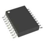 SN74LV8T245QDGSRQ1

The activity of extra discounts on wholesale prices is in full swing…
Please fill in your contact information and we will send you the latest wholesale price list.





