 ChipApex | Global Electronic Components Supplier

SEARCH
Search Product
Search Post
— IC芯片 | 连接器 | 传感器 | 被动器件 —
Search productSearch post
— IC芯片 | 连接器 | 传感器 | 被动器件 —
Consult the customer manager about the wholesale price.
consultation hotline:86-132-6715-2157
email:[email protected]
Contact the product manager for consultation. One-stop consultation is available.
Do you want a lower wholesale price? Please send us your inquiry and we will reply immediately.
SN74LVC125APWG4 is listed in the Buffers, Drivers, Receivers, Transceivers range at ChipApex. The manufacturer field lists Texas Instruments. Its product description is IC BUF NON-INVERT 3.6V 14TSSOP. Review the specifications below when checking this part for your BOM.
The SN74LVC125APWG4 is a quadruple bus buffer gate with 3-state outputs manufactured by Texas Instruments. It operates from a supply voltage of 1.65V to 3.6V and features independent output-enable inputs for each buffer. The device accepts input voltages up to 5.5V, allowing compatibility with mixed 3.3V/5V systems. It is housed in a 14-pin TSSOP package and supports operating temperatures from -40°C to 85°C or -40°C to 125°C.
Verify the specific suffix 'G4' indicates RoHS compliance and green manufacturing options as per Texas Instruments standards. Confirm the PW package designation corresponds to the 14-pin Thin Shrink Small Outline Package (TSSOP). Ensure the selected temperature grade matches the required operational environment limits defined in the datasheet specifications.
Select this component when designing circuits requiring bus buffering between logic families operating at different voltage levels, specifically translating between 3.3V and 5V domains. The independent output enables allow precise control over bus contention. Consider the maximum propagation delay and drive current capabilities relative to the load capacitance and signal integrity requirements of the target application.
This part belongs to the SN74LVC125A family of quadruple bus buffer gates. The 'PW' suffix identifies the 14-pin TSSOP physical package, while the 'G4' suffix denotes environmental compliance attributes including lead-free finish and RoHS adherence. It is a production-active component within the Texas Instruments logic IC portfolio.
SN74LVC125ADBRG4
To ensure the high-impedance state during power up or power down, the OE input should be tied to VCC through a pull-up resistor.
Each output is disabled when the associated output-enable (OE) input is high. When OE is low, the respective gate passes data from the A input to its Y output.
Explore related parts through Logic, Integrated Circuits (ICs), all product categories, ChipApex homepage.
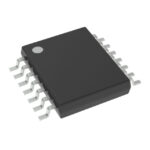 SN74LVC125APWG4

The activity of extra discounts on wholesale prices is in full swing…
Please fill in your contact information and we will send you the latest wholesale price list.





