 ChipApex | Global Electronic Components Supplier
SEARCH
Search Product
Search Post
— IC芯片 | 连接器 | 传感器 | 被动器件 —
Search productSearch post
— IC芯片 | 连接器 | 传感器 | 被动器件 —
Consult the customer manager about the wholesale price.
consultation hotline:86-132-6715-2157
email:[email protected]
Contact the product manager for consultation. One-stop consultation is available.
Do you want a lower wholesale price? Please send us your inquiry and we will reply immediately.
The SN74LVC138AMPWTEP is a 3-line to 8-line decoder and demultiplexer from Texas Instruments' LVC logic family. It operates within a supply voltage range of 1.65 V to 3.6 V, ensuring compatibility with low-voltage digital systems. The device features a propagation delay of 6.7 ns and functions reliably across an industrial temperature range from -40°C to +85°C. Packaged in a 16-pin TSSOP format, it provides eight active-low outputs controlled by three binary inputs and three enable pins.
Verify the specific suffix 'EP' indicates enhanced product specifications or packaging variations compared to standard variants. Confirm the TSSOP-16 package dimensions match your PCB footprint requirements. Ensure the operating temperature range aligns with your environmental constraints. Cross-reference the datasheet revision date to confirm current electrical characteristics before finalizing component selection.
Select this component when low-power consumption and high-speed switching are required in compact designs. The LVC series offers improved performance over older logic families while maintaining pin compatibility. Consider the TSSOP package for surface-mount applications requiring higher pin density. Verify that the input voltage levels are compatible with your system's logic thresholds.
This part belongs to the SN74LVC138A family of decoders and demultiplexers manufactured by Texas Instruments. The LVC series is designed for low-voltage applications, offering faster switching speeds and lower power dissipation compared to traditional CMOS logic. The 'AMPWTEP' designation specifies the automotive-grade or enhanced performance variant in a TSSOP package, distinguishing it from standard commercial versions.
Compatible substitutes include the SN74LVC138APWR and SN74LVC138ADRE4. Verify that alternative packages such as SOIC or PW (TSSOP) meet your mechanical constraints. Ensure the substitute maintains the same LVC logic family characteristics for voltage and speed compatibility.
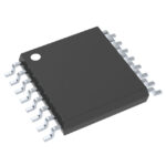 SN74LVC138AMPWTEP
The activity of extra discounts on wholesale prices is in full swing…
Please fill in your contact information and we will send you the latest wholesale price list.






