 ChipApex | Global Electronic Components Supplier
SEARCH
Search Product
Search Post
— IC芯片 | 连接器 | 传感器 | 被动器件 —
Search productSearch post
— IC芯片 | 连接器 | 传感器 | 被动器件 —
Consult the customer manager about the wholesale price.
consultation hotline:86-132-6715-2157
email:[email protected]
Contact the product manager for consultation. One-stop consultation is available.
Do you want a lower wholesale price? Please send us your inquiry and we will reply immediately.
The SN74LVC139ADRG4 is a dual 2-line to 4-line decoder/demultiplexer from the Texas Instruments LVC logic family. It operates within a supply voltage range of 1.65 V to 3.6 V and supports an operating temperature range of -40 °C to +85 °C. The device features fully buffered inputs that accept voltages up to 5.5 V, enabling compatibility with 3.3-V or 5-V driving circuits. It provides a maximum propagation delay of 6.2 ns at 3.3 V and includes ESD protection exceeding 2000 V per the human-body model.
Verify the specific ordering suffix 'RGY' corresponds to the VQFN package variant when sourcing. Confirm RoHS compliance and lead finish specifications against current manufacturer documentation. Ensure the active-low enable polarity matches system design requirements. Validate thermal pad soldering guidelines for the selected package type during assembly planning.
Choose this component for applications requiring low-voltage operation down to 1.65 V with high-speed decoding capabilities. The 5.5 V tolerant inputs simplify interface design in environments mixing different logic families. Consider the dual-structure efficiency for space-constrained designs needing two separate decoding channels within a single footprint.
This part belongs to the SN74LVC139A series, representing a generation of low-voltage CMOS logic designed for modern portable and battery-powered electronics. The LVC family bridges the gap between traditional 5-V TTL compatibility and emerging sub-3-V power domains, offering improved power efficiency while maintaining robust noise immunity.
SN74LVC139ADR (SOIC Package)
Yes, the active-low enable (G) input can be utilized as a data line specifically for demultiplexing applications.
Yes, the fully buffered inputs accept voltages up to 5.5 V, allowing direct interfacing with 5-V devices while operating at lower supply voltages.
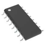 SN74LVC139ADRG4
The activity of extra discounts on wholesale prices is in full swing…
Please fill in your contact information and we will send you the latest wholesale price list.





