 ChipApex | Global Electronic Components Supplier
SEARCH
Search Product
Search Post
— IC芯片 | 连接器 | 传感器 | 被动器件 —
Search productSearch post
— IC芯片 | 连接器 | 传感器 | 被动器件 —
Consult the customer manager about the wholesale price.
consultation hotline:86-132-6715-2157
email:[email protected]
Contact the product manager for consultation. One-stop consultation is available.
Do you want a lower wholesale price? Please send us your inquiry and we will reply immediately.
The SN74LVC139APW is a dual 2-line to 4-line decoder/demultiplexer from the Texas Instruments LVC logic family. It operates within a supply voltage range of 1.65 V to 3.6 V and features active-low enable inputs that function as data lines in demultiplexing applications. The device incorporates fully buffered inputs compatible with 3.3-V or 5-V driving circuits, facilitating translation in mixed-voltage systems. It provides a maximum propagation delay of 6.2 ns and includes ESD protection exceeding JESD 22 standards.
Verify the specific ordering suffix against the manufacturer's current Package Option Addendum to confirm the exact packaging configuration. Confirm RoHS compliance status and moisture sensitivity level ratings prior to procurement. Ensure the selected variant matches the required tape-and-reel or tube quantity specifications for the intended assembly process.
Select this component when designing low-voltage logic circuits requiring simultaneous decoding of two address lines. The LVC series is appropriate for portable applications due to its wide operating voltage range. Verify that the TSSOP-16 package dimensions align with the printed circuit board layout constraints and thermal management requirements of the target design.
This part belongs to the SN74LVC139A family of dual decoders manufactured by Texas Instruments. It utilizes advanced CMOS technology optimized for low-power operation across varying supply voltages. The PW suffix specifically denotes the Thin-Shrink Small Outline Package (TSSOP) housing, which offers a compact footprint suitable for high-density surface-mount assemblies.
Direct substitutes include other variants within the SN74LVC139A family such as SN74LVC139ADBR or SN74LVC139ADR, provided the package type change is accommodated by the PCB design. Cross-manufacturer equivalents require verification of pinout compatibility and electrical parameter alignment.
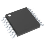 SN74LVC139APW
The activity of extra discounts on wholesale prices is in full swing…
Please fill in your contact information and we will send you the latest wholesale price list.





