 ChipApex | Global Electronic Components Supplier
SEARCH
Search Product
Search Post
— IC芯片 | 连接器 | 传感器 | 被动器件 —
Search productSearch post
— IC芯片 | 连接器 | 传感器 | 被动器件 —
Consult the customer manager about the wholesale price.
consultation hotline:86-132-6715-2157
email:[email protected]
Contact the product manager for consultation. One-stop consultation is available.
Do you want a lower wholesale price? Please send us your inquiry and we will reply immediately.
The SN74LVC139AZQNR is a dual 2-line to 4-line decoder/demultiplexer from the LVC family. It operates from 1.65 V to 3.6 V with inputs accepting voltages up to 5.5 V. The device features active-low enable inputs usable as data lines, fully buffered inputs representing one normalized load, and latch-up performance exceeding 250 mA per JESD 17. ESD protection exceeds JESD 22 standards. It is housed in a ZQN package (VFBGA) and supports an operating temperature range of -40°C to 85°C.
Verify the specific ZQN package variant matches your PCB footprint requirements. Confirm the voltage levels align with your system's I/O standards. Ensure proper handling procedures are followed due to moisture sensitivity. Check for automotive qualification if required for your application environment.
Select this component when low voltage operation between 1.65 V and 3.6 V is required. Consider its ability to interface with 5-V logic despite lower supply voltages. Evaluate the ZQN package size against available board space. Verify thermal management needs for the chosen operating conditions.
This part belongs to Texas Instruments' LVC logic family, designed for low-voltage digital applications. It provides high-speed decoding capabilities while maintaining compatibility with standard logic interfaces. The ZQN package offers a compact solution for space-constrained designs requiring reliable signal routing.
SN74LVC139ARGYR
Yes, the active-low enable inputs can function as data lines in demultiplexing configurations.
Yes, the inputs accept voltages up to 5.5 V, allowing direct interfacing with 5-V devices even when powered at lower voltages.
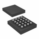 SN74LVC139AZQNR
The activity of extra discounts on wholesale prices is in full swing…
Please fill in your contact information and we will send you the latest wholesale price list.





