 ChipApex | Global Electronic Components Supplier

SEARCH
Search Product
Search Post
— IC芯片 | 连接器 | 传感器 | 被动器件 —
Search productSearch post
— IC芯片 | 连接器 | 传感器 | 被动器件 —
Consult the customer manager about the wholesale price.
consultation hotline:86-132-6715-2157
email:[email protected]
Contact the product manager for consultation. One-stop consultation is available.
Do you want a lower wholesale price? Please send us your inquiry and we will reply immediately.
SN74LVC165APWR is listed in the Shift Registers range at ChipApex. The manufacturer field lists Texas Instruments. Its product description is 1.1V TO 3.6V PARALLEL-LOAD EIGHT. Review the specifications below when checking this part for your BOM.
The SN74LVC165APWR is an 8-bit parallel-load shift register from the LVC logic family, manufactured by Texas Instruments. It operates within a supply voltage range of 1.1V to 3.6V and features over-voltage tolerant inputs supporting up to 5.5V independent of VCC. The device provides high push-pull output drive strength and supports partial-power-down with back-drive protection (Ioff). It includes a serial input for daisy-chaining capabilities and offers both standard and inverted serial outputs.
Verify that the ordering suffix matches the required package type, as the base part number covers multiple physical packages. Confirm the specific temperature grade and electrical characteristics align with the design requirements before procurement. Ensure the component meets all relevant RoHS standards and functional safety ratings if applicable to the target application environment.
Select this component when a low-voltage parallel-to-serial conversion is required with minimal pin count usage. Consider the LVC series for compatibility with modern low-voltage logic families. Evaluate the propagation delay specifications against the system clock frequency to ensure timing margins are met during the shifting process.
This component belongs to the SN74LVC165A family of 8-bit parallel-load shift registers. The 'PWR' suffix specifically denotes the TSSOP-16 surface-mount package variant. This family is designed for applications requiring efficient data serialization from parallel sources while maintaining low power consumption and robust performance across varying supply voltages.
SN74LVC165ADWR
The device includes circuitry to disable all outputs when the supply pin is held at 0V. In this state, outputs neither source nor sink current regardless of applied input voltages, preventing back-driving.
The CLK INH pin acts as a clock inhibit input. Clocking is inhibited when this pin is high. It can be used interchangeably with the CLK pin for triggering shifts, provided the transition levels are managed correctly relative to the other clock signal.
Explore related parts through Logic, Integrated Circuits (ICs), all product categories, ChipApex homepage.
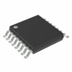 SN74LVC165APWR

The activity of extra discounts on wholesale prices is in full swing…
Please fill in your contact information and we will send you the latest wholesale price list.





