 ChipApex | Global Electronic Components Supplier
SEARCH
Search Product
Search Post
— IC芯片 | 连接器 | 传感器 | 被动器件 —
Search productSearch post
— IC芯片 | 连接器 | 传感器 | 被动器件 —
Consult the customer manager about the wholesale price.
consultation hotline:86-132-6715-2157
email:[email protected]
Contact the product manager for consultation. One-stop consultation is available.
Do you want a lower wholesale price? Please send us your inquiry and we will reply immediately.
The SN74LVC257APWRE4 is a quadruple 2-line to 1-line data selector and multiplexer with 3-state outputs. It operates from 1.65V to 3.6V VCC, accepts inputs up to 5.5V, and features a maximum propagation delay of 4.6ns at 3.3V. The device provides ESD protection exceeding 2000V (HBM) and latch-up performance over 250mA. Packaged in TSSOP-16, it supports mixed 3.3V/5V system environments.
Verify the specific suffix 'E4' indicates RoHS compliance and manufacturing location details as defined by Texas Instruments. Confirm the package type matches the required PCB footprint. Ensure the ordering quantity aligns with the reel specifications provided in the packaging addendum. Cross-reference the datasheet revision date to confirm current parameter validity before finalizing procurement.
Select this component when designing bus-organized systems requiring signal multiplexing between 4-bit data sources and output lines. It is suitable for applications needing level translation between 3.3V and 5V devices. Consider the 4.6ns maximum propagation delay for timing constraints. Verify that the 3-state outputs meet the bus loading requirements of the target system architecture.
This part belongs to the SNx4LVC257A family of quadruple 2-line to 1-line data selectors. It utilizes CMOS technology to provide balanced output drive capabilities. The device is designed specifically for low-voltage digital signal processing applications where space efficiency and voltage compatibility are critical design factors.
SN74LVC257APWR
The inputs accept voltages up to 5.5V, allowing them to be driven directly by 3.3V or 5V devices. This enables the SN74LVC257APWRE4 to function effectively as a translator in mixed 3.3V and 5V system environments.
To ensure proper device operation and prevent undefined states, all unused inputs must be held at VCC or GND. Floating inputs should be avoided as they can lead to excessive power consumption or erratic behavior.
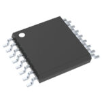 SN74LVC257APWRE4
The activity of extra discounts on wholesale prices is in full swing…
Please fill in your contact information and we will send you the latest wholesale price list.






