 ChipApex | Global Electronic Components Supplier
SEARCH
Search Product
Search Post
— IC芯片 | 连接器 | 传感器 | 被动器件 —
Search productSearch post
— IC芯片 | 连接器 | 传感器 | 被动器件 —
Consult the customer manager about the wholesale price.
consultation hotline:86-132-6715-2157
email:[email protected]
Contact the product manager for consultation. One-stop consultation is available.
Do you want a lower wholesale price? Please send us your inquiry and we will reply immediately.
The SN74LVC257AQDREP is a quad 2-input multiplexer from Texas Instruments, designed for high-speed digital signal routing. It operates within a supply voltage range of 2V to 3.6V and features three-state outputs to prevent bus loading when disabled. The device provides a maximum propagation delay of 4.6ns at 3.3V and supports output currents of 24mA. It is housed in a 16-SOIC package and meets automotive standards with an operating temperature range of -55°C to +125°C.
Verify the specific suffix 'REP' indicates enhanced product or military grade specifications as per official documentation. Confirm RoHS compliance status and ensure the 16-SOIC package dimensions match your PCB footprint requirements. Check for any recent Product Change Notices regarding manufacturing location or material composition updates before finalizing procurement.
Select this component for applications requiring robust automotive-grade logic switching. Ensure the system voltage remains within the 2V to 3.6V range to maintain specified timing parameters. Consider the 16-SOIC package size for space-constrained designs. Verify that the input voltage levels are compatible with the driving source logic family to guarantee reliable signal integrity across the full temperature range.
This part belongs to the SN74LVC257A series of quad multiplexers. The 'AQ' designation typically signifies automotive qualification, while 'REP' often denotes a specific reliability or enhanced product variant. It serves as a digital switch for routing data signals in complex electronic systems, offering high density and speed compared to standard logic families.
The maximum propagation delay is 4.6ns when operating at a supply voltage of 3.3V.
Yes, the SN74LVC257AQDREP features three-state outputs, which allow the device to disconnect from the bus when disabled.
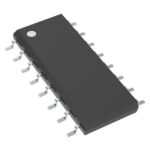 SN74LVC257AQDREP
The activity of extra discounts on wholesale prices is in full swing…
Please fill in your contact information and we will send you the latest wholesale price list.





