 ChipApex | Global Electronic Components Supplier
SEARCH
Search Product
Search Post
— IC芯片 | 连接器 | 传感器 | 被动器件 —
Search productSearch post
— IC芯片 | 连接器 | 传感器 | 被动器件 —
Consult the customer manager about the wholesale price.
consultation hotline:86-132-6715-2157
email:[email protected]
Contact the product manager for consultation. One-stop consultation is available.
Do you want a lower wholesale price? Please send us your inquiry and we will reply immediately.
The SN74LVC257AQPWRQ1 is an automotive-grade quadruple 2-line to 1-line data selector/multiplexer with 3-state outputs. It operates from a supply voltage of 2V to 3.6V and accepts input voltages up to 5.5V. The device features a maximum propagation delay of 4.6ns at 3.3V. ESD protection exceeds 2000V per MIL-STD-883, method 3015. It is designed for bus-organized systems where 3-state outputs prevent loading when the output-enable input is high.
Verify the specific package type (TSSOP, SOIC, or WQFN) required for your design, as the SN74LVC257A-Q1 family includes multiple physical configurations. Confirm that the AEC-Q100 qualification aligns with your automotive reliability standards. Ensure proper bypass capacitor placement near VCC terminals during implementation to maintain signal integrity.
Select this component when designing for automotive environments requiring robust ESD protection and mixed-voltage interface capabilities. The 5.5V tolerant inputs allow direct interfacing with legacy 5V logic without level shifters. Consider the thermal characteristics and package options based on your PCB layout constraints and heat dissipation requirements.
This part belongs to the SN74LVC257A-Q1 series, which are automotive-qualified versions of the standard LVC logic family. The 'Q1' suffix denotes automotive qualification. Other variants include catalog versions like SN74LVC257A and military versions like SN54LVC257A, offering different performance levels and environmental ratings.
SN74LVC257APWRQ1
When the Output Enable (OE) input is at a high logic level, the 3-state outputs enter a high-impedance state, preventing them from loading the data lines.
Unused inputs must not be left floating. They should be connected to either VCC or GND to prevent undefined operational states caused by undefined voltages.
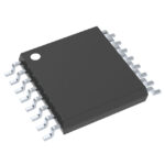 SN74LVC257AQPWRQ1
The activity of extra discounts on wholesale prices is in full swing…
Please fill in your contact information and we will send you the latest wholesale price list.





