 ChipApex | Global Electronic Components Supplier

SEARCH
Search Product
Search Post
— IC芯片 | 连接器 | 传感器 | 被动器件 —
Search productSearch post
— IC芯片 | 连接器 | 传感器 | 被动器件 —
Consult the customer manager about the wholesale price.
consultation hotline:86-132-6715-2157
email:[email protected]
Contact the product manager for consultation. One-stop consultation is available.
Do you want a lower wholesale price? Please send us your inquiry and we will reply immediately.
SN74S240NE4 is listed in the Buffers, Drivers, Receivers, Transceivers range at ChipApex. The manufacturer field lists Texas Instruments. Its product description is 8-CH, 4.75-V TO 5.25-V BIPOLAR I. Review the specifications below when checking this part for your BOM.
The SN74S240NE4 is an octal buffer and line driver manufactured by Texas Instruments, utilizing Schottky transistor logic technology. It features two independent 4-bit drivers with inverted outputs and active-low output-enable inputs (G). The device provides three-state outputs capable of driving bus lines or buffering memory address registers. It operates within a supply voltage range of 4.75 V to 5.25 V and supports an operating temperature range of 0 °C to 70 °C. The component is housed in a 20-pin PDIP package.
Verify the specific ordering suffix against the manufacturer's current documentation to confirm package type and environmental compliance. Ensure the procurement channel sources from authorized distributors to guarantee authenticity. Confirm that the component meets the required RoHS standards for your manufacturing process. Check for any updates to the datasheet revision history regarding parameter changes.
Select this component when high-speed data transmission is required due to its fast propagation delay characteristics. It is suitable for mixed 3.3-V and 5-V system environments as inputs are tolerant down to 2 V. Consider the high fan-out and improved fan-in capabilities for complex bus-oriented receiver and transmitter designs.
This part belongs to the SNx4S24x family of octal buffers and line drivers. It shares functional similarities with the SN74LS240 but utilizes Schottky technology for faster switching speeds. The 'NE4' suffix typically denotes a lead-free, environmentally compliant version of the standard SN74S240 in a PDIP-20 package.
SN74S240N
To ensure the high-impedance state during power up or power down, the G pin must be tied to VCC through a pullup resistor.
The G pins are active-low output-enable inputs. When G is low, the device passes data from the A inputs to the Y outputs; when G is high, the outputs enter a high impedance state.
Explore related parts through Logic, Integrated Circuits (ICs), all product categories, ChipApex homepage.
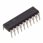 SN74S240NE4

The activity of extra discounts on wholesale prices is in full swing…
Please fill in your contact information and we will send you the latest wholesale price list.





