 ChipApex | Global Electronic Components Supplier

SEARCH
Search Product
Search Post
— IC芯片 | 连接器 | 传感器 | 被动器件 —
Search productSearch post
— IC芯片 | 连接器 | 传感器 | 被动器件 —
Consult the customer manager about the wholesale price.
consultation hotline:86-132-6715-2157
email:[email protected]
Contact the product manager for consultation. One-stop consultation is available.
Do you want a lower wholesale price? Please send us your inquiry and we will reply immediately.
SN74SSTU32864CZKER is listed in the Specialty Logic range at ChipApex. The manufacturer field lists Texas Instruments. Its product description is IC 25BIT CONFIG REG BUFF 96-BGA. Review the specifications below when checking this part for your BOM.
The SN74SSTU32864CZKER is a 25-bit configurable registered buffer with SSTL_18 inputs and outputs, designed for 1.7-V to 1.9-V VCC operation. It supports differential clock (CLK and CLK) inputs and LVCMOS switching levels on family control and RESET inputs. The device can be configured as a 25-bit 1:1 or 14-bit 1:2 registered buffer. It features chip-select inputs to minimize system power consumption and output edge-control circuitry to minimize switching noise in unterminated lines. The package is LFBGA-ZKE with 96 pins.
Verify the specific ordering suffix ZKER corresponds to the LFBGA-ZKE package and tape-and-reel packing configuration. Confirm the device status is PREVIEW or ACTIVE as per the latest Texas Instruments documentation before finalizing procurement plans. Ensure compatibility with SSTL_18 voltage levels and differential clock requirements for the target application design.
Select this component when designing systems requiring a configurable registered buffer for DDR2 memory interfaces. Consider the 1:1 versus 1:2 pinout configurations based on the number of SDRAM loads required per DIMM. Evaluate the low-power standby and active modes if power efficiency is a critical design constraint. Ensure the design accommodates the differential clock inputs and LVCMOS control signals.
This part belongs to the Texas Instruments Widebus+ series of logic ICs. It is specifically engineered for high-density memory applications, providing flexibility in buffer configuration to optimize PCB layout for DDR2 DIMMs. The device integrates advanced features like edge-controlled outputs and chip-select functionality to enhance signal integrity and power management in complex digital systems.
Check for SN74SSTU32864CGKER as an alternative package option within the same functional family. Verify pinout compatibility and electrical specifications before substituting. Consult Texas Instruments for any newer generations or direct replacements that may offer improved performance or availability.
When the RESET input is low, the differential input receivers are disabled, all registers are reset, and all outputs are forced low. This ensures defined outputs from the register before a stable clock has been supplied.
The C0 and C1 inputs control the pinout configuration. C0 selects between Register A and Register B configurations in the 1:2 mode, while C1 selects between the 25-bit 1:1 and 14-bit 1:2 configurations. These inputs should be hard-wired and not switched during normal operation.
Yes, the device supports low-power standby operation when RESET is low, disabling differential input receivers. It also supports low-power active operation by monitoring DCS and CSR inputs, which can gate Qn outputs from changing states to minimize power consumption.
Explore related parts through Logic, Integrated Circuits (ICs), all product categories, ChipApex homepage.
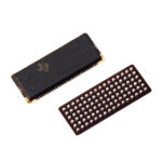 SN74SSTU32864CZKER

The activity of extra discounts on wholesale prices is in full swing…
Please fill in your contact information and we will send you the latest wholesale price list.






