 ChipApex | Global Electronic Components Supplier

SEARCH
Search Product
Search Post
— IC芯片 | 连接器 | 传感器 | 被动器件 —
Search productSearch post
— IC芯片 | 连接器 | 传感器 | 被动器件 —
Consult the customer manager about the wholesale price.
consultation hotline:86-132-6715-2157
email:[email protected]
Contact the product manager for consultation. One-stop consultation is available.
Do you want a lower wholesale price? Please send us your inquiry and we will reply immediately.
SN74SSTU32866GKER is listed in the Specialty Logic range at ChipApex. The manufacturer field lists Texas Instruments. Its product description is IC 25BIT CONFIG REG BUFF 96LFBGA. Review the specifications below when checking this part for your BOM.
The SN74SSTU32866GKER is a 25-bit 1:1 or 14-bit 1:2 configurable registered buffer designed for 1.7-V to 1.9-V VCC operation. It features SSTL_18 data inputs and LVCMOS control inputs, with edge-controlled outputs optimized for unterminated DIMM loads. The device supports differential clock inputs (CLK and CLK) and includes parity checking on DIMM-independent data inputs via the PAR_IN pin. It allows cascading with a second SN74SSTU32866 for expanded parity monitoring.
Verify the GKE package suffix corresponds to the LFBGA form factor and tape-and-reel packing. Confirm the operating temperature range matches the 0°C to 70°C specification. Ensure the design accounts for the specific pinout configurations required for 1:1 versus 1:2 modes, particularly regarding unused DNU pins.
Select this component when designing DDR2 RDIMMs requiring configurable bus width and integrated parity checking. It is suitable for applications needing edge-controlled outputs to minimize switching noise on unterminated lines. Consider cascading capabilities if extended parity monitoring across multiple devices is required.
Part of the Texas Instruments Widebus+ family, the SN74SSTU32866 is optimized for DDR2 DIMM PCB layout. It provides a flexible solution for memory buffering by allowing configuration between 25-bit and 14-bit widths through hard-wired C0 and C1 inputs.
SN74SSTU32866GKER
Explore related parts through Logic, Integrated Circuits (ICs), all product categories, ChipApex homepage.
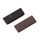 SN74SSTU32866GKER

The activity of extra discounts on wholesale prices is in full swing…
Please fill in your contact information and we will send you the latest wholesale price list.






