 ChipApex | Global Electronic Components Supplier

SEARCH
Search Product
Search Post
— IC芯片 | 连接器 | 传感器 | 被动器件 —
Search productSearch post
— IC芯片 | 连接器 | 传感器 | 被动器件 —
Consult the customer manager about the wholesale price.
consultation hotline:86-132-6715-2157
email:[email protected]
Contact the product manager for consultation. One-stop consultation is available.
Do you want a lower wholesale price? Please send us your inquiry and we will reply immediately.
SN74SSTUB32864NMJR is listed in the Specialty Logic range at ChipApex. The manufacturer field lists Texas Instruments. Its product description is IC CONFIG REG BUFF 25BIT 96-BGA. Review the specifications below when checking this part for your BOM.
The SN74SSTUB32864NMJR is a 25-bit configurable register buffer manufactured by Texas Instruments. It operates with a supply voltage range of 1.7V to 1.9V and features SSTL_18 compliant outputs optimized for unterminated DIMM loads. The device supports differential clock inputs (CLK and CLK) and includes LVCMOS control inputs for reset and configuration. It provides low-power standby and active modes via dedicated control signals, ensuring glitch-free operation during power-up and reset transitions.
Verify the specific suffix NMJR against the manufacturer's current datasheet to confirm package type and tape-and-reel specifications. Ensure that the operating voltage constraints of 1.7V to 1.9V align with the target system's power delivery network. Confirm that the required reset and configuration pin hardwiring matches the final hardware design before procurement.
Select this component when designing DDR2 RDIMMs that require driving up to nine SDRAM loads per device in a 1:1 configuration. Choose the 1:2 configuration if the design requires driving eighteen loads using two devices per DIMM. Ensure the design can accommodate the requirement for differential clock inputs and that the C0 and C1 configuration pins can be hardwired to fixed logic levels.
This device belongs to the SN74SSTV family of buffers and line drivers from Texas Instruments. It is specifically engineered for memory interface applications, providing the necessary buffering and timing control for synchronous DRAM systems. The part integrates both data registration and output driving capabilities into a single compact package.
Public confirmed substitute part numbers only; omit otherwise.
To ensure defined outputs before stable clocks are provided, the RESET input must be held low during power-up. This clears the registers and forces outputs low, preventing glitches until the differential input receivers are fully enabled.
C1 controls the pin configuration between 25-bit 1:1 (low) and 14-bit 1:2 (high). C0 controls the pin configuration between Register A (low) and Register B (high) in the 1:2 arrangement. These should be hardwired and not switched during normal operation.
Explore related parts through Logic, Integrated Circuits (ICs), all product categories, ChipApex homepage.
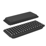 SN74SSTUB32864NMJR

The activity of extra discounts on wholesale prices is in full swing…
Please fill in your contact information and we will send you the latest wholesale price list.






