 ChipApex | Global Electronic Components Supplier
SEARCH
Search Product
Search Post
— IC芯片 | 连接器 | 传感器 | 被动器件 —
Search productSearch post
— IC芯片 | 连接器 | 传感器 | 被动器件 —
Consult the customer manager about the wholesale price.
consultation hotline:86-132-6715-2157
email:[email protected]
Contact the product manager for consultation. One-stop consultation is available.
Do you want a lower wholesale price? Please send us your inquiry and we will reply immediately.
The SN74V215-7PAG is a high-speed, low-power CMOS synchronous FIFO memory with a 512 x 18-bit organization. It supports clock frequencies up to 133 MHz and features read-access times as fast as 5 ns. The device operates on a +3.3-V supply with 5-V input tolerance. It includes programmable almost-empty and almost-full flags, half-full flag capability, and supports both first-word fall-through and standard timing modes.
Verify the specific suffix 'PAG' corresponds to the 64-pin Thin Quad Flat Package configuration. Confirm that the '-7' speed grade meets the required system timing constraints. Ensure the component matches the 3.3-V VCC specification and 5-V tolerant input requirements for your target logic family.
Select this component when a 512 x 18-bit synchronous buffer is required for high-speed data transfer. It is suitable for designs needing independent read/write clocks and programmable flag thresholds. Consider the 64-pin TQFP package dimensions for PCB layout compatibility.
This part belongs to the SN74V215/225/235/245 family of DSP-Sync FIFO memories. While other variants offer different depths such as 1024, 2048, or 4096 words, the SN74V215 specifically provides the 512-word capacity. All members share identical pinouts and functional descriptions regarding flag logic and expansion capabilities.
SN74V215-10PAG
In FWFT mode, the first word written to an empty FIFO appears on the outputs after three RCLK transitions without requiring a Read Enable assertion. In Standard mode, a specific read operation using REN is required to shift the first word to the outputs.
The Load (LD) pin controls access to the internal offset registers. When LD is low, data on inputs D0–D11 writes to the offset registers on the WCLK edge, allowing users to program the almost-empty and almost-full flag thresholds.
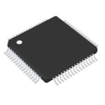 SN74V215-7PAG
The activity of extra discounts on wholesale prices is in full swing…
Please fill in your contact information and we will send you the latest wholesale price list.





