 ChipApex | Global Electronic Components Supplier
SEARCH
Search Product
Search Post
— IC芯片 | 连接器 | 传感器 | 被动器件 —
Search productSearch post
— IC芯片 | 连接器 | 传感器 | 被动器件 —
Consult the customer manager about the wholesale price.
consultation hotline:86-132-6715-2157
email:[email protected]
Contact the product manager for consultation. One-stop consultation is available.
Do you want a lower wholesale price? Please send us your inquiry and we will reply immediately.
The SN74V3660-6PEU is a 3.3-V CMOS first-in, first-out (FIFO) memory with a 4096 × 36 bit organization and 128-pin TQFP package. It supports 166-MHz operation with a 6-ns read/write cycle time. The device features user-selectable bus sizing for input and output ports at widths of 36, 18, or 9 bits. It includes big-endian/little-endian selectable byte representation, 5-V tolerant inputs, and fixed low first-word latency. The FIFO offers zero-latency retransmit, master reset, partial reset, and programmable almost-empty/full flags.
Verify the specific ordering suffix matches the required package type and temperature range. Confirm that the revision level aligns with current production data specifications. Ensure compatibility with system voltage levels and interface requirements before finalizing procurement decisions.
Select this component when a deep, high-speed FIFO with flexible bus matching is required. Consider the 4096-word depth and 36-bit width capabilities. Evaluate the need for independent clock domains and programmable flag offsets. Verify that the 128-pin TQFP package fits the design constraints.
This part belongs to the SN74V36xx series of 3.3-V CMOS FIFO memories from Texas Instruments. The series includes variants with different depths ranging from 1024 to 32768 words, all maintaining a 36-bit word width. These devices are designed for high-performance submicron CMOS technology applications.
Compatible substitutes within the same family include SN74V3640, SN74V3650, SN74V3670, SN74V3680, and SN74V3690. Selection depends on required memory depth. All variants share identical pinouts and functional characteristics except for storage capacity.
Bus width is configured using the BM, IW, and OW pins during the master reset cycle to select input and output widths of 36, 18, or 9 bits.
In standard mode, every read requires REN and RCLK. In FWFT mode, the first word appears automatically after three RCLK edges without REN, while subsequent words require REN.
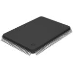 SN74V3660-6PEU
The activity of extra discounts on wholesale prices is in full swing…
Please fill in your contact information and we will send you the latest wholesale price list.





