 ChipApex | Global Electronic Components Supplier

SEARCH
Search Product
Search Post
— IC芯片 | 连接器 | 传感器 | 被动器件 —
Search productSearch post
— IC芯片 | 连接器 | 传感器 | 被动器件 —
Consult the customer manager about the wholesale price.
consultation hotline:86-132-6715-2157
email:[email protected]
Contact the product manager for consultation. One-stop consultation is available.
Do you want a lower wholesale price? Please send us your inquiry and we will reply immediately.
SNJ54ABT543AFK is listed in the Buffers, Drivers, Receivers, Transceivers range at ChipApex. The manufacturer field lists Texas Instruments. Its product description is OCTAL REGISTERED TRANSCEIVER WIT. Review the specifications below when checking this part for your BOM.
The SNJ54ABT543AFK is an octal registered transceiver utilizing state-of-the-art EPIC-II BiCMOS design. It features two sets of D-type latches for temporary data storage and bidirectional flow control. The device operates within a supply voltage range of 4.5 V to 5.5 V and supports high-drive outputs with -32-mA IOH and 64-mA IOL capabilities. It is characterized for operation over the full military temperature range of -55°C to 125°C.
Verify that the component matches the SNJ54ABT543AFK designation specifically for military-grade specifications. Confirm the package type corresponds to the Ceramic Chip Carrier (FK) variant. Ensure the operating environment aligns with the -55°C to 125°C temperature range requirements. Check for QML certification if required by specific defense contracts.
Select this component when bidirectional data transfer with internal latching is necessary in harsh environments. The FK package is suitable for applications requiring ceramic construction. Consider the high-drive output capability for driving heavy loads. Verify compatibility with 5-V logic families given the specified input and output voltage levels.
This part belongs to the SN54ABT543A family of octal registered transceivers. The 'SNJ' prefix indicates a military-grade device, while the 'FK' suffix denotes the 28-pin Ceramic Chip Carrier package. It is distinct from the commercial SN74ABT543A series which has a narrower temperature range.
SN54ABT543AWD
CEAB controls the A-to-B data flow direction, while LEAB enables the A latches to enter storage mode upon a low-to-high transition.
To ensure a high-impedance state during power transitions, the OE input should be tied to VCC through a pullup resistor.
Explore related parts through Logic, Integrated Circuits (ICs), all product categories, ChipApex homepage.
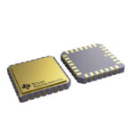 SNJ54ABT543AFK

The activity of extra discounts on wholesale prices is in full swing…
Please fill in your contact information and we will send you the latest wholesale price list.





