 ChipApex | Global Electronic Components Supplier

SEARCH
Search Product
Search Post
— IC芯片 | 连接器 | 传感器 | 被动器件 —
Search productSearch post
— IC芯片 | 连接器 | 传感器 | 被动器件 —
Consult the customer manager about the wholesale price.
consultation hotline:86-132-6715-2157
email:[email protected]
Contact the product manager for consultation. One-stop consultation is available.
Do you want a lower wholesale price? Please send us your inquiry and we will reply immediately.
The SNJ54BCT541FK is an octal buffer and line driver featuring three-state outputs, manufactured using state-of-the-art BiCMOS technology. It operates within a supply voltage range of 4.5 V to 5.5 V and supports an operating temperature range from -55°C to 125°C. The device utilizes a 20-pin LCCC (FK) package. Key electrical characteristics include a maximum propagation delay of 8.7 ns at 5 V with a 50 pF load, low input clamp current, and high output drive capability.
Verify the specific ordering suffix FK corresponds to the Leadless Ceramic Chip Carrier package configuration. Confirm military-grade qualification requirements if applicable, as indicated by the SNJ prefix. Ensure compatibility with MIL-PRF-38535 standards for critical applications where full parameter testing is mandated rather than production processing assumptions.
Select this component for designs requiring octal buffering with independent dual output enable controls. The BiCMOS technology offers a balance between speed and power consumption suitable for high-density logic applications. Consider the through-hole pinout arrangement when designing PCB footprints to optimize trace routing efficiency compared to standard parallel I/O configurations.
This part belongs to the BCT family of octal buffers and drivers. It shares functional similarities with the SN54BCT541 series but is distinguished by its specific ceramic packaging and extended temperature rating. The device serves as a non-inverting buffer, providing signal isolation and amplification for digital logic levels within complex integrated circuits.
SNJ54BCT541J
To ensure the high-impedance state during power-up or power-down, the OE inputs should be tied to VCC through a pullup resistor.
The 3-state control gate consists of a 2-input AND gate with active-low inputs; if either OE1 or OE2 is high, all eight outputs enter the high-impedance state.
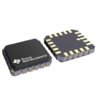 SNJ54BCT541FK

The activity of extra discounts on wholesale prices is in full swing…
Please fill in your contact information and we will send you the latest wholesale price list.





