 ChipApex | Global Electronic Components Supplier

SEARCH
Search Product
Search Post
— IC芯片 | 连接器 | 传感器 | 被动器件 —
Search productSearch post
— IC芯片 | 连接器 | 传感器 | 被动器件 —
Consult the customer manager about the wholesale price.
consultation hotline:86-132-6715-2157
email:[email protected]
Contact the product manager for consultation. One-stop consultation is available.
Do you want a lower wholesale price? Please send us your inquiry and we will reply immediately.
The SNJ54HC365J is a military-grade hex buffer and line driver featuring six independent buffers with three-state outputs. It operates within a supply voltage range of 2 V to 6 V and supports an operating temperature range from -55 °C to 125 °C. The device utilizes a 16-pin ceramic dual in-line package (CDIP). Key electrical characteristics include high-current outputs capable of driving up to 15 LSTTL loads, low power consumption with a maximum ICC of 80 µA, and typical propagation delays of 10 ns.
Verify the specific ordering suffix 'J' corresponds to the 16-lead CDIP package configuration. Confirm that the military qualification status aligns with project requirements. Ensure compatibility with existing board layouts designed for the specified pinout and thermal characteristics.
Select this component when high-density bus buffering is required in harsh environments. The HC logic family offers improved speed and lower power compared to older standards. Verify that the input transition times remain within recommended limits to ensure proper switching performance at the target supply voltage.
This part belongs to the SN54HC365 series, which is the military-qualified version of the commercial SN74HC365. Both share identical logical functionality but differ in manufacturing standards and environmental testing protocols. The SN54 variant is certified for extended temperature ranges and reliability standards required for defense applications.
SN54HC365J
The outputs enter a high-impedance state if either OE1 or OE2 is set to a high state. Data passes from A inputs to Y outputs only when both enable pins are low.
The SNJ54HC365J is housed in a 16-lead Ceramic Dual In-Line Package (CDIP).
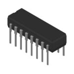 SNJ54HC365J

The activity of extra discounts on wholesale prices is in full swing…
Please fill in your contact information and we will send you the latest wholesale price list.





