 ChipApex | Global Electronic Components Supplier
SEARCH
Search Product
Search Post
— IC芯片 | 连接器 | 传感器 | 被动器件 —
Search productSearch post
— IC芯片 | 连接器 | 传感器 | 被动器件 —
Consult the customer manager about the wholesale price.
consultation hotline:86-132-6715-2157
email:[email protected]
Contact the product manager for consultation. One-stop consultation is available.
Do you want a lower wholesale price? Please send us your inquiry and we will reply immediately.
The SNJ54S195J is a 4-bit parallel-access shift register manufactured by Texas Instruments. It features a dual clock system with separate inputs for serial data and clock pulses, enabling flexible data shifting operations. The device operates within a military-grade temperature range of -55°C to 125°C and utilizes a 16-pin ceramic dual in-line package (CDIP). Key electrical characteristics include an operating voltage range of 4.5V to 5.5V. It supports both serial-in/parallel-out and parallel-in/serial-out configurations through dedicated control pins.
Verify the component suffix 'J' confirms the ceramic DIP package and military temperature rating. Ensure the datasheet matches the specific revision for pinout accuracy. Confirm compliance with export control classifications if applicable. Validate that the source document explicitly lists this part number to avoid confusion with similar plastic packages or commercial grade variants.
Select this component when military-grade temperature tolerance and ceramic package durability are required. The dual-clock design offers timing flexibility compared to single-clock alternatives. Consider the 4-bit width for simple shift applications rather than larger registers. Verify power supply constraints align with the specified 4.5V to 5.5V range before integration into the circuit design.
This part belongs to the SN54xx series of logic integrated circuits, which are distinguished by their extended temperature ranges and robust construction suitable for aerospace and defense applications. Unlike the SN74xx commercial series, the SN54xx series ensures functionality across wider thermal extremes. The SNJ54S195J specifically implements Schottky TTL technology for improved speed and power efficiency relative to standard TTL devices.
The serial clock controls the shifting of data into the flip-flops one bit at a time, while the parallel clock enables the simultaneous loading of data from the parallel inputs into the register.
Yes, the parallel load function can be disabled, allowing the device to operate solely as a serial-in/serial-out or serial-in/parallel-out shift register based on the control pin states.
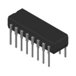 SNJ54S195J
The activity of extra discounts on wholesale prices is in full swing…
Please fill in your contact information and we will send you the latest wholesale price list.





