 ChipApex | Global Electronic Components Supplier

SEARCH
Search Product
Search Post
— IC芯片 | 连接器 | 传感器 | 被动器件 —
Search productSearch post
— IC芯片 | 连接器 | 传感器 | 被动器件 —
Consult the customer manager about the wholesale price.
consultation hotline:86-132-6715-2157
email:[email protected]
Contact the product manager for consultation. One-stop consultation is available.
Do you want a lower wholesale price? Please send us your inquiry and we will reply immediately.
SSTUA32866EC/G,518 is listed in the Specialty Logic range at ChipApex. The manufacturer field lists NXP USA Inc.. Its product description is IC REG BUFFER 25BIT 96-LFBGA. Review the specifications below when checking this part for your BOM.
The SSTUA32866EC/G,518 is a 1.8 V configurable registered buffer designed for DDR2 memory modules requiring parity checking. It operates within a supply voltage range of 1.7 V to 2.0 V and supports clock frequencies up to 450 MHz. The device features a maximum single-bit switching propagation delay of 1.8 ns and a mass-switching delay of 2.0 ns. It provides low-level output current of 8 mA and high-level output current of -8 mA. The component is housed in a 96-ball LFBGA package with dimensions of 13.5 mm x 5.5 mm.
Verify the specific ordering suffix matches the required solder ball compound, as EC denotes lead-free SnAgCu while other variants may use SnPb. Confirm the package version corresponds to the SOT536-1 designation. Ensure the ambient temperature rating aligns with the specified commercial range of 0 °C to +70 °C for the intended application environment.
Select this component when designing DDR2 registered memory solutions that mandate parity verification capabilities. The choice depends on the required topology, either a full 25-bit width or a split 14-bit configuration for dual-register setups. Consider the power consumption characteristics and the specific timing requirements relative to the memory controller interface speed.
This part belongs to the NXP SSTU series of configurable registered buffers. It is specifically engineered to meet JEDEC standards for DDR2 applications. The device integrates both buffering and error-checking logic into a single package, reducing the component count compared to separate buffer and parity check ICs.
SSTUA32866EC/S,518
Explore related parts through Logic, Integrated Circuits (ICs), all product categories, ChipApex homepage.
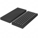 SSTUA32866EC/G,518

The activity of extra discounts on wholesale prices is in full swing…
Please fill in your contact information and we will send you the latest wholesale price list.






