 ChipApex | Global Electronic Components Supplier

SEARCH
Search Product
Search Post
— IC芯片 | 连接器 | 传感器 | 被动器件 —
Search productSearch post
— IC芯片 | 连接器 | 传感器 | 被动器件 —
Consult the customer manager about the wholesale price.
consultation hotline:86-132-6715-2157
email:[email protected]
Contact the product manager for consultation. One-stop consultation is available.
Do you want a lower wholesale price? Please send us your inquiry and we will reply immediately.
SY100EL16VDKG is listed in the Specialty Logic range at ChipApex. The manufacturer field lists Microchip Technology. Its product description is IC RCVR DIFF 5V/3.3V 10-MSOP. Review the specifications below when checking this part for your BOM.
The SY100EL16VDKG is an enhanced differential receiver from the SY10/100EL16VA-VF series, manufactured by Microchip Technology. It operates with 3.3V and 5V power supplies and features a 10-pin MSOP package. The device provides data synchronous enable/disable functionality for glitchless gating of high-gain outputs. Key electrical parameters include a propagation delay of up to 780 ps at +85°C, a minimum input swing of 150 mV, and a common mode range of -1.4 V to -0.4 V.
Verify the specific ordering suffix 'KG' corresponds to the industrial temperature range and Pb-free NiPdAu finish as documented in the manufacturer's ordering information table. Confirm the 10-pin MSOP package type matches the design requirements. Ensure compatibility with existing PCB footprints for the K10-1 package format before finalizing procurement decisions.
Select this component when glitchless output gating is required for crystal oscillator or timing signal applications. The SY100EL16VDKG variant specifically combines the enable input feature with the 10-pin MSOP package option. Consider the high DC gain of the QHG outputs if signal amplification is needed alongside reception. Verify that the 3.3V or 5V supply options align with the system power architecture.
This part belongs to the SY10/100EL16VA-VF family of enhanced differential receivers. The 'VD' suffix indicates the inclusion of both Q and /Q outputs along with the /EN enable input, packaged in a 10-pin MSOP format. It serves as a specialized solution for high-frequency timing applications requiring precise control over output states without introducing glitches during enable transitions.
SY100EL16VDZC (16-pin SOIC, same function)
The /EN input synchronizes with the data input to provide glitchless gating. When /EN is LOW, data passes through. When /EN goes HIGH, it forces specific output states on the next negative data transition, disabling further output changes while /EN remains HIGH.
The QHG and /QHG outputs have a DC gain several times larger than the DC gain of the standard Q and /Q outputs, making them suitable for applications requiring higher voltage gain.
Explore related parts through Logic, Integrated Circuits (ICs), all product categories, ChipApex homepage.
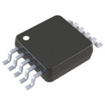 SY100EL16VDKG

The activity of extra discounts on wholesale prices is in full swing…
Please fill in your contact information and we will send you the latest wholesale price list.





