 ChipApex | Global Electronic Components Supplier

SEARCH
Search Product
Search Post
— IC芯片 | 连接器 | 传感器 | 被动器件 —
Search productSearch post
— IC芯片 | 连接器 | 传感器 | 被动器件 —
Consult the customer manager about the wholesale price.
consultation hotline:86-132-6715-2157
email:[email protected]
Contact the product manager for consultation. One-stop consultation is available.
Do you want a lower wholesale price? Please send us your inquiry and we will reply immediately.
SY100EP11UKG-TR is listed in the Clock Buffers, Drivers range at ChipApex. The manufacturer field lists Microchip Technology. Its product description is IC CLK BUFFER 1:2 3GHZ 8MSOP. Review the specifications below when checking this part for your BOM.
The SY100EP11UKG-TR is a precision, high-speed 1:2 differential fanout buffer from the ECL Pro™ family. It supports 2.5V, 3.3V, and 5V power supplies for PECL, LVPECL, ECL, and LVECL operation. The device features guaranteed AC parameters including a maximum toggle frequency exceeding 3.0GHz, output-to-output skew under 20ps, and propagation delay under 300ps. It is housed in an 8-pin MSOP package with industrial temperature range (-40°C to +85°C) and lead-free NiPdAu finish.
Verify that the ordering suffix 'KG' corresponds to the Pb-Free package with NiPdAu finish and Industrial temperature range as specified in the datasheet. Confirm the 'TR' suffix indicates Tape and Reel packaging. Ensure the design accounts for the specific DC electrical characteristics at the intended VCC voltage (2.5V, 3.3V, or 5V).
Select this component when low skew and high-frequency operation (>3GHz) are critical. Compare against the SY10EP11U variant if commercial temperature range is sufficient. Ensure termination resistors match the selected VCC level (e.g., R1=130Ω/R2=82Ω for 3.3V/5V) to maintain signal integrity.
This part belongs to the Micrel SY10/100EP11U series of differential fanout buffers. It serves as an upgrade to the EL11V, offering improved within-device skews and output transition times. The '100' prefix typically denotes the industrial temperature grade compared to the '10' commercial grade.
Public confirmed substitute part numbers include MC10EP11D/DT and MC10LVEP11D/DT from ON Semiconductor. Verify pinout and electrical specifications before substitution.
If the inputs are left open, the Q outputs will go LOW due to the internal clamping circuitry.
Single-ended input CLK pin operation is limited to VCC ≥ 3.0V in PECL mode and VEE ≤ -3.0V in ECL/LVECL mode.
For a 3.3V system, use R1 = 130Ω and R2 = 82Ω for Thevenin termination, or Rb = 46Ω to 50Ω for Y-termination.
Explore related parts through Clock/Timing, Integrated Circuits (ICs), all product categories, ChipApex homepage.
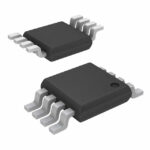 SY100EP11UKG-TR

The activity of extra discounts on wholesale prices is in full swing…
Please fill in your contact information and we will send you the latest wholesale price list.






