 ChipApex | Global Electronic Components Supplier

SEARCH
Search Product
Search Post
— IC芯片 | 连接器 | 传感器 | 被动器件 —
Search productSearch post
— IC芯片 | 连接器 | 传感器 | 被动器件 —
Consult the customer manager about the wholesale price.
consultation hotline:86-132-6715-2157
email:[email protected]
Contact the product manager for consultation. One-stop consultation is available.
Do you want a lower wholesale price? Please send us your inquiry and we will reply immediately.
SY100EP14UK4G is listed in the Clock Buffers, Drivers range at ChipApex. The manufacturer field lists Microchip Technology. Its product description is IC CLK BUFFER 2:5 2GHZ 20TSSOP. Review the specifications below when checking this part for your BOM.
The SY100EP14UK4G is a high-speed, 2 GHz differential PECL/ECL 1:5 fanout buffer optimized for ultra-low skew applications. It features a 2:1 input multiplexer and operates within a wide supply voltage range of 2.37V to 5.5V. The device guarantees less than 25ps within-device skew over temperature and supply voltage variations. Inputs accept PECL, LVPECL, ECL, LVECL, and HSTL logic levels, while outputs provide fully differential signals compatible with 100K ECL standards. It includes an integrated VBB reference for single-ended or AC-coupled inputs and a synchronous enable pin to prevent runt clock pulses.
Verify the industrial temperature rating (-40°C to +85°C) and K4 package marking (XEP14U). Confirm RoHS compliance via the Pb-Free bar line indicator on the component body. Ensure proper termination resistors are used for the specific supply voltage configuration.
Select this component when interfacing between different logic families such as HSTL, LVPECL, and ECL. Use the internal VBB reference for AC-coupled single-ended inputs to eliminate external resistor networks. Ensure the application requires a 1:5 output ratio and supports differential signaling.
This part belongs to Micrel's Precision Edge® and ECL Pro™ high-speed clock synchronization family. It is manufactured by Microchip Technology following the acquisition of Micrel. The 'G' suffix indicates a lead-free package variant recommended for new designs.
Consult the manufacturer website for other devices in the high-speed, low-skew fanout buffer, translator, and clock generator product lines if different I/O combinations are required.
Connect the VBB pin to the unused /CLK pin and bypass it to VCC through a 0.01µF capacitor.
The /EN pin is a synchronous enable that forces outputs into a fixed logic state only after the outputs are in a LOW state, preventing runt clock pulses.
/CLK0 and /CLK1 default to VCC/2, while CLK0 and CLK1 default to LOW due to internal pull-down resistors.
Explore related parts through Clock/Timing, Integrated Circuits (ICs), all product categories, ChipApex homepage.
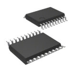 SY100EP14UK4G

The activity of extra discounts on wholesale prices is in full swing…
Please fill in your contact information and we will send you the latest wholesale price list.





