 ChipApex | Global Electronic Components Supplier

SEARCH
Search Product
Search Post
— IC芯片 | 连接器 | 传感器 | 被动器件 —
Search productSearch post
— IC芯片 | 连接器 | 传感器 | 被动器件 —
Consult the customer manager about the wholesale price.
consultation hotline:86-132-6715-2157
email:[email protected]
Contact the product manager for consultation. One-stop consultation is available.
Do you want a lower wholesale price? Please send us your inquiry and we will reply immediately.
SY100S834ZI is listed in the Clock Generators, PLLs, Frequency Synthesizers range at ChipApex. The manufacturer field lists Microchip Technology. Its product description is IC CLOCK GENERATOR 16SOIC. Review the specifications below when checking this part for your BOM.
The SY100S834ZI is a low skew clock generation chip from the Precision Edge series, manufactured by Micrel (now Microchip Technology). It provides synchronous divide-by-1, ÷2, and ÷4 outputs when the Function Select (FSEL) pin is high, or ÷2, ÷4, and ÷8 outputs when FSEL is low. The device supports differential or single-ended ECL/PECL inputs and operates within an industrial temperature range of -40°C to +85°C. Key electrical parameters include a maximum output-to-output skew of 50ps, a typical propagation delay of 1100ps, and a power supply current of approximately 49mA.
Verify component authenticity through authorized channels as this part originates from Micrel, which was acquired by Microchip Technology. Confirm that the specific ordering suffix 'ZI' corresponds to the Industrial temperature range (-40°C to +85°C) and the Z16-2 package type. Ensure compatibility with existing system voltage levels and logic families before procurement.
Select the SY100S834ZI over the SY100S834L variant if operation at 5V power supplies is required, as the L version is optimized for 3.3V. Consider the FSEL pin configuration to determine if ÷1 or ÷8 outputs are needed for the specific frequency multiplication or division requirements of the design.
This component belongs to the SY100S834/L family of clock generators. It is designed explicitly for applications demanding minimal skew between multiple clock outputs derived from a single source. The device integrates internal dividers that are synchronous to each other, ensuring common output edges are precisely aligned.
The SY100S834LZI serves as a lower-voltage alternative operating at 3.3V. For lead-free compliance in new designs, the SY100S834ZG variant offers NiPdAu finish instead of Sn-Pb, though functional specifications remain identical.
When FSEL is LOW, the device generates ÷2, ÷4, and ÷8 outputs. When FSEL is HIGH, it generates ÷1, ÷2, and ÷4 outputs, effectively doubling the maximum output frequency capability.
The VBB pin acts as a reference output. For single-ended input conditions, it should be connected to the CLK input and bypassed to ground via a 0.01µF capacitor to serve as the switching reference.
No, the enable (EN) function is synchronous. Internal dividers are only enabled or disabled when the internal clock is in the LOW state to prevent runt pulses and maintain synchronization.
Explore related parts through Clock/Timing, Integrated Circuits (ICs), all product categories, ChipApex homepage.
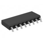 SY100S834ZI

The activity of extra discounts on wholesale prices is in full swing…
Please fill in your contact information and we will send you the latest wholesale price list.







