 ChipApex | Global Electronic Components Supplier
SEARCH
Search Product
Search Post
— IC芯片 | 连接器 | 传感器 | 被动器件 —
Search productSearch post
— IC芯片 | 连接器 | 传感器 | 被动器件 —
Consult the customer manager about the wholesale price.
consultation hotline:86-132-6715-2157
email:[email protected]
Contact the product manager for consultation. One-stop consultation is available.
Do you want a lower wholesale price? Please send us your inquiry and we will reply immediately.
The SY55856UHG is a SuperLite differential two-channel precision CML delay line manufactured by Microchip Technology. It operates within a supply voltage range of 2.3V to 3.6V and supports maximum frequencies exceeding 2.5GHz with a throughput up to 5Gbps. The device provides a total adjustable delay range of ±350ps in 50ps increments, controlled via three digital select pins. It features source-terminated CML outputs optimized for 50Ω loads, delivering a 400mV differential swing. Propagation delay is guaranteed at less than 384ps, with rise/fall times under 120ps. The component is housed in a 32-pin EPAD-TQFP package and functions across an industrial temperature range from -40°C to +85°C.
Verify the specific ordering suffix to confirm the package type and lead finish. The 'HG' suffix indicates a Pb-Free variant with NiPdAu finish. Confirm that the procurement channel sources the correct tape and reel quantity if applicable. Ensure the supplier provides valid RoHS compliance documentation matching the specific manufacturing batch.
Select this component when precise relative timing adjustments are required between differential signals. Ensure the system design accommodates the 2.3V to 3.6V supply range and utilizes appropriate 50Ω source termination for the CML outputs. Verify that the control interface logic levels match the LVL pin configuration requirements.
This part belongs to the SuperLite family of high-speed analog and digital crosspoint ICs originally developed by Micrel, which was acquired by Microchip Technology. The series focuses on precision timing and signal routing solutions for telecommunications and networking applications requiring low jitter and fast switching speeds.
Check for updated Microchip datasheets as the original manufacturer notes this part is not recommended for new designs. Evaluate alternative devices from the same family or newer generations that offer equivalent delay ranges and CML specifications while supporting current manufacturing standards.
The DELAY_SEL pin determines whether the clock signal is delayed relative to the data signal or vice versa. A logic high delays the clock, while a logic low delays the data.
The LVL pin sets the voltage threshold for the variable threshold inputs (S0, S1, S2, DELAY_SEL, CINV), allowing the device to interface with different logic families like TTL or PECL.
Yes, the CINV pin allows for optional inversion of the CLK_IN signal, resulting in an inverted CLK_OUT output when driven above the threshold voltage.
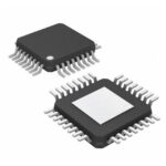 SY55856UHG
The activity of extra discounts on wholesale prices is in full swing…
Please fill in your contact information and we will send you the latest wholesale price list.





