 ChipApex | Global Electronic Components Supplier

SEARCH
Search Product
Search Post
— IC芯片 | 连接器 | 传感器 | 被动器件 —
Search productSearch post
— IC芯片 | 连接器 | 传感器 | 被动器件 —
Consult the customer manager about the wholesale price.
consultation hotline:86-132-6715-2157
email:[email protected]
Contact the product manager for consultation. One-stop consultation is available.
Do you want a lower wholesale price? Please send us your inquiry and we will reply immediately.
SY58013UMG-TR is listed in the Clock Buffers, Drivers range at ChipApex. The manufacturer field lists Microchip Technology. Its product description is IC CLK BUFFER 1:2 6GHZ 16MLF. Review the specifications below when checking this part for your BOM.
The SY58013UMG-TR is a Precision Edge® 1:2 fanout buffer and translator manufactured by Microchip Technology. It features 400mV LVPECL outputs with internal input termination, supporting clock frequencies up to 6GHz and data rates up to 10.7Gbps. The device accepts differential inputs from LVPECL, LVDS, or CML sources via a unique VT pin architecture. Key electrical parameters include a maximum propagation delay of 250ps, channel-to-channel skew under 15ps, and typical RMS phase jitter of 55fs. It operates on a single supply voltage ranging from 2.375V to 3.6V within an industrial temperature range of -40°C to +85°C.
Verify that the component is sourced from authorized distributors to ensure authenticity. Confirm RoHS compliance status and check for specific manufacturing lot codes if required for traceability. Ensure proper ESD handling procedures are followed during storage and assembly due to the high-speed nature of the device.
Select the SY58013UMG-TR when a 1:2 fanout buffer with 400mV LVPECL outputs is required. Choose this part over the SY58011U if LVPECL compatibility is needed instead of CML, or over the SY58012U if lower output swing (400mV vs 800mV) is acceptable. Ensure the design can accommodate the internal input termination requirements via the VT pin.
This component belongs to Micrel’s (now Microchip's) Precision Edge® product line of high-speed logic devices. It is functionally similar to the SY58011U and SY58012U but specifically optimized for 400mV LVPECL outputs. The 'TR' suffix indicates the device is supplied in tape and reel packaging for automated surface-mount assembly.
The SY58011UMG-TR offers CML outputs instead of LVPECL. The SY58012UMG-TR provides 800mV LVPECL outputs. Verify output voltage levels and interface compatibility before substituting these parts.
For AC-coupled inputs, connect the VREF-AC pin directly to the VT pin. The VREF-AC pin biases to VCC – 1.2V and should be bypassed with a 0.01µF low ESR capacitor to VCC.
Unused output pairs (Q and /Q) may be left floating without impacting jitter. If balancing is required, terminate the unused pair using the parallel termination network described in the datasheet.
Yes, the device accepts LVDS differential signals. The unique 3-pin input termination architecture allows it to interface with LVDS, LVPECL, and CML signals without external level-shifting networks.
Explore related parts through Clock/Timing, Integrated Circuits (ICs), all product categories, ChipApex homepage.
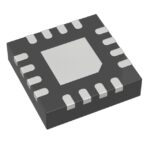 SY58013UMG-TR

The activity of extra discounts on wholesale prices is in full swing…
Please fill in your contact information and we will send you the latest wholesale price list.




