 ChipApex | Global Electronic Components Supplier

SEARCH
Search Product
Search Post
— IC芯片 | 连接器 | 传感器 | 被动器件 —
Search productSearch post
— IC芯片 | 连接器 | 传感器 | 被动器件 —
Consult the customer manager about the wholesale price.
consultation hotline:86-132-6715-2157
email:[email protected]
Contact the product manager for consultation. One-stop consultation is available.
Do you want a lower wholesale price? Please send us your inquiry and we will reply immediately.
SY58607UMG is listed in the Clock Buffers, Drivers range at ChipApex. The manufacturer field lists Microchip Technology. Its product description is IC CLK BUFFER 1:2 3GHZ 16MLF. Review the specifications below when checking this part for your BOM.
The SY58607UMG is a high-speed, fully differential 1:2 LVPECL fanout buffer from Microchip Technology. It processes clock signals up to 2.5 GHz or data patterns up to 3.2 Gbps with guaranteed AC performance across the industrial temperature range of –40°C to +85°C. The device features an ultra-low jitter design with 41 fs additive phase jitter and less than 20 ps within-device skew. It operates on a 2.5V ±5% or 3.3V ±10% supply voltage and includes fail-safe input functionality to prevent output oscillation during invalid input conditions.
Verify the specific ordering suffix for packaging requirements. The standard tube configuration contains 100 units per tube. Alternatively, the -TR suffix indicates a tape and reel configuration containing 1,000 units per reel. Confirm package availability directly with the manufacturer or authorized sales offices as distribution options may vary.
Select the SY58607UMG for applications requiring 800 mV LVPECL outputs. For designs needing CML or LVDS outputs instead, consider the SY58606U (400 mV swing) or SY58608U (325 mV swing). Ensure the power supply matches the required 2.5V ±5% or 3.3V ±10% specifications to maintain the guaranteed electrical characteristics.
The SY58607UMG belongs to Microchip’s Precision Edge® product line of high-speed logic devices. Originally developed by Micrel, this component was integrated into Microchip's portfolio following their acquisition. The part number designation 'U' indicates dual voltage support, while 'M' specifies the 16-lead QFN package.
For alternative output swings within the same family, consider the SY58606U for 400 mV CML/LVDS outputs or the SY58608U for 325 mV LVDS outputs. These parts share similar form factors but differ in output voltage levels and interface compatibility.
The FSI circuit senses the input signal amplitude. If the signal drops below approximately 100 mVpk (typically 30 mVpk), it latches the outputs to their last valid state, preventing metastability or oscillation.
The device supports data rates up to 3.2 Gbps (NRZ) and clock frequencies up to 2.5 GHz (with VOUT > 400 mV).
Yes, the differential input accepts DC-coupled signals as small as 100 mV (200 mVpp) without requiring level-shifting or external termination resistor networks in the signal path.
Explore related parts through Clock/Timing, Integrated Circuits (ICs), all product categories, ChipApex homepage.
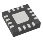 SY58607UMG

The activity of extra discounts on wholesale prices is in full swing…
Please fill in your contact information and we will send you the latest wholesale price list.




