 ChipApex | Global Electronic Components Supplier

SEARCH
Search Product
Search Post
— IC芯片 | 连接器 | 传感器 | 被动器件 —
Search productSearch post
— IC芯片 | 连接器 | 传感器 | 被动器件 —
Consult the customer manager about the wholesale price.
consultation hotline:86-132-6715-2157
email:[email protected]
Contact the product manager for consultation. One-stop consultation is available.
Do you want a lower wholesale price? Please send us your inquiry and we will reply immediately.
SY75572LMG is listed in the Clock Buffers, Drivers range at ChipApex. The manufacturer field lists Microchip Technology. Its product description is IC CLK BUFFER 2:2 267MHZ 16QFN. Review the specifications below when checking this part for your BOM.
The SY75572LMG is a high-speed, fully differential 1:2 clock fanout buffer from Microchip Technology. It features two pairs of differential inputs and outputs supporting HCSL or LVDS logic levels. The device operates on a 3.3V ±5% supply (3.135V to 3.465V) within the industrial temperature range of –40°C to +85°C. It supports a maximum frequency of 267 MHz for HCSL and 100 MHz for LVDS. Key electrical parameters include ultra-low phase jitter (137 fs RMS at 200 MHz), less than 2 ps total jitter (peak-to-peak), and 50 ps output-to-output skew. It is housed in a 16-pin QFN package.
Verify the ordering suffix to confirm packaging configuration. The 'G' suffix indicates an industrial temperature range (-40°C to +85°C). The base part number SY75572LMG typically denotes tube packaging, while the '-TR' suffix designates tape and reel packaging containing 1,000 units. Confirm the specific package variant required for the assembly process.
Select this component when low jitter distribution is critical for high-speed interfaces like PCIe. Ensure the input signal matches the supported HCSL or LVDS voltage levels. Note that the LVDS mode is limited to a maximum frequency of 100 MHz, whereas HCSL supports up to 267 MHz. Verify that the PCB layout accommodates the 16-pin QFN package dimensions.
The SY75572LMG belongs to Microchip’s PrecisionEdge™ product line of high-speed, ultra-low jitter buffers. It is designed to replace legacy buffering solutions in datacom and telecom infrastructure where signal integrity is paramount. The device provides two identical output copies derived from one of two selectable differential inputs.
Public confirmed substitute part numbers are not available in the provided documentation.
When configured for LVDS logic levels, the SY75572LMG supports a maximum frequency of 100 MHz.
The device includes a 2:1 input multiplexer. The SEL pin determines the active input pair: Logic High selects IN1, while Logic Low selects IN2.
The typical power supply current (IDD) is 42 mA under standard load conditions (50Ω, 2 pF).
Explore related parts through Clock/Timing, Integrated Circuits (ICs), all product categories, ChipApex homepage.
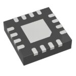 SY75572LMG

The activity of extra discounts on wholesale prices is in full swing…
Please fill in your contact information and we will send you the latest wholesale price list.






