 ChipApex | Global Electronic Components Supplier
SEARCH
Search Product
Search Post
— IC芯片 | 连接器 | 传感器 | 被动器件 —
Search productSearch post
— IC芯片 | 连接器 | 传感器 | 被动器件 —
Consult the customer manager about the wholesale price.
consultation hotline:86-132-6715-2157
email:[email protected]
Contact the product manager for consultation. One-stop consultation is available.
Do you want a lower wholesale price? Please send us your inquiry and we will reply immediately.
The SY89296UTG is a programmable delay line from the Precision Edge® series, manufactured by Microchip Technology. It operates on a 2.5V ±5% or 3.3V ±10% power supply and supports frequencies up to 1.5GHz. The device provides a programmable delay range of 3.2ns to 14.8ns in 10ps increments using a 10-bit control word, with an additional fine-tune capability via the FTUNE pin for approximately 40ps continuous adjustment. It features LVPECL differential inputs and outputs, low jitter performance (<10ps PP total), and is available in a 32-pin TQFP package.
Verify that the ordering suffix 'UTG' corresponds to the lead-free NiPdAu finish and the 32-pin TQFP package type as specified in the manufacturer's ordering information. Confirm compatibility with industrial operating temperatures ranging from -40°C to +85°C. Ensure design requirements align with the specific Pb-Free package recommendations for new designs.
Select the SY89296UTG when analog fine-tuning of the delay is required, distinguishing it from the SY89295U which lacks the FTUNE pin. Consider the 32-pin TQFP package if through-hole or standard surface-mount assembly methods are preferred over the MLF variant. Verify that the input signal swing and logic levels match the supported LVPECL, CMOS, or LVTTL specifications.
The SY89296UTG belongs to Micrel’s (now Microchip) high-speed Precision Edge product line. It serves as an enhanced version of the SY89295U by adding analog fine-tune control capabilities. This component is designed for applications requiring precise timing alignment in high-frequency clock distribution networks.
The SY89295U is a related part within the same family but lacks the FTUNE pin for analog fine-tuning. Designers requiring only discrete step delays may consider this alternative, though functional differences regarding fine-tuning must be evaluated.
The IN and /IN pins default to an equivalent low state when left floating. Similarly, the D control bits contain pull-downs and default LOW when unconnected.
The VBB pin provides an internally generated reference voltage output. It is used to bias the unused input of a differential pair when using a single-ended source or to re-bias AC-coupled inputs.
Yes, two or more devices can be cascaded using the D10 bit and the Cascade/CASCADE outputs to extend the total delay range.
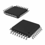 SY89296UTG
The activity of extra discounts on wholesale prices is in full swing…
Please fill in your contact information and we will send you the latest wholesale price list.





