 ChipApex | Global Electronic Components Supplier
SEARCH
Search Product
Search Post
— IC芯片 | 连接器 | 传感器 | 被动器件 —
Search productSearch post
— IC芯片 | 连接器 | 传感器 | 被动器件 —
Consult the customer manager about the wholesale price.
consultation hotline:86-132-6715-2157
email:[email protected]
Contact the product manager for consultation. One-stop consultation is available.
Do you want a lower wholesale price? Please send us your inquiry and we will reply immediately.
The SY89306VMI-TR is a high-speed differential buffer/receiver manufactured by Microchip Technology. It operates at frequencies up to 2.5 GHz with a typical propagation delay of 100 ps and duty cycle skew of 8 ps. The device supports 3.3 V to 5.5 V power supplies, drawing a maximum supply current of 48 mA. It features 100K PECL/ECL compatible inputs and outputs, including internal 75 kΩ pull-down resistors on the D and /D pins. The component is housed in an ultra-small 8-lead 2 mm x 2 mm DFN package and functions within an industrial temperature range of –40°C to +85°C.
Verify the specific ordering suffix 'TR' corresponds to the tape and reel packaging configuration containing 1,000 units per reel. Confirm that the 'M' package designation matches the required 8-lead DFN footprint for your PCB layout. Ensure the 'G' suffix indicates the specified industrial temperature range and lead finish before finalizing procurement orders.
Select this component when space constraints require an 8-lead DFN package instead of larger alternatives like the SY100EL16V. Choose this part if the design requires integrated input pull-down resistors to simplify termination networks. Verify that the operating voltage range of 3.0 V to 5.5 V aligns with the system power rails and that the 48 mA maximum current draw fits the thermal budget.
This device belongs to the SY89 series of high-speed differential receivers and buffers from Microchip Technology. It serves as a compact alternative to legacy parts such as the SY100EL16V, offering a significantly smaller footprint while maintaining functional equivalence. The product line focuses on providing robust signal integrity solutions for high-frequency digital communication interfaces.
The SY88927V is functionally equivalent but lacks the reduced footprint advantage. Designers replacing older SY100EL16V components should verify that the 8-lead DFN package dimensions are compatible with existing board layouts or tooling.
Under open input conditions where the inputs are pulled to VEE, internal input clamps force the Q output to a LOW state.
The VBB pin provides a bias voltage of approximately VCC - 1.32 V. It must be bypassed to ground via a 0.01 μF capacitor and can only source or sink a maximum of 0.5 mA.
The maximum frequency is guaranteed for functionality at 2.5 GHz, provided the output voltage swing is at least 400 mV.
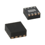 SY89306VMI TR
The activity of extra discounts on wholesale prices is in full swing…
Please fill in your contact information and we will send you the latest wholesale price list.





