 ChipApex | Global Electronic Components Supplier

SEARCH
Search Product
Search Post
— IC芯片 | 连接器 | 传感器 | 被动器件 —
Search productSearch post
— IC芯片 | 连接器 | 传感器 | 被动器件 —
Consult the customer manager about the wholesale price.
consultation hotline:86-132-6715-2157
email:[email protected]
Contact the product manager for consultation. One-stop consultation is available.
Do you want a lower wholesale price? Please send us your inquiry and we will reply immediately.
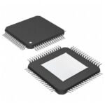
SY89825UHI is listed in the Clock Buffers, Drivers range at ChipApex. The manufacturer field lists Microchip Technology. Its product description is IC CLK BUFFER 2:22 2GHZ 64TQFP. Review the specifications below when checking this part for your BOM.
The SY89825UHI is a high-performance bus clock driver and translator manufactured by Microchip Technology, originally designed by Micrel. It features one differential input multiplexed between LVDS and LVPECL, providing 22 differential LVPECL output pairs. The device operates on a single supply voltage ranging from 2.37V to 3.6V. Key electrical specifications include a maximum toggle frequency of 2 GHz, a maximum channel-to-channel skew of 35 ps, and a total jitter of 10 ps peak-to-peak. The LVDS input includes an internal 100Ω termination. It is housed in a 64-pin exposed pad TQFP package.
The SY89825UHI is marked as obsolete and no longer manufactured. Verification should confirm component authenticity and physical condition upon receipt. Solderability and lead finish (Sn-Pb) must be inspected against storage guidelines. Designers are advised to utilize the recommended Pb-free replacement part for new designs due to RoHS compliance requirements.
Select this component when a single-chip solution is required to distribute a clock signal to up to 22 destinations with precise alignment. It is suitable for environments requiring low skew (<35 ps) and operation at frequencies up to 2 GHz. Ensure the design accommodates the 64-TQFP package dimensions and thermal dissipation requirements, particularly regarding the exposed pad connection to ground.
This device belongs to the Precision Edge® series of clock drivers. Originally developed by Micrel, Inc., the product line was acquired by Microchip Technology. The SY89825U family is engineered for low-voltage, high-speed clock distribution where minimizing part-to-part skew and reducing board space compared to multi-device solutions are critical design constraints.
The SY89825UHY is listed as a direct replacement. The primary difference is the lead finish: the UHI uses Sn-Pb, while the UHY utilizes Matte-Sn and includes a Pb-Free bar-line indicator. Pinouts and functionality remain identical, facilitating drop-in substitution for existing assemblies.
The input source is selected using the CLK_SEL pin. When CLK_SEL is Low, the LVDS inputs are active; when High, the LVPECL inputs are active.
The OE pin is synchronized with the clock signal to ensure outputs are only enabled or disabled when they are already in the LOW state, preventing the generation of runt clock pulses.
No, the LVDS input includes an internal 100Ω termination between the LVDS_CLK and /LVDS_CLK pins.
Explore related parts through Clock/Timing, Integrated Circuits (ICs), all product categories, ChipApex homepage.
 SY89825UHI

The activity of extra discounts on wholesale prices is in full swing…
Please fill in your contact information and we will send you the latest wholesale price list.




