 ChipApex | Global Electronic Components Supplier

SEARCH
Search Product
Search Post
— IC芯片 | 连接器 | 传感器 | 被动器件 —
Search productSearch post
— IC芯片 | 连接器 | 传感器 | 被动器件 —
Consult the customer manager about the wholesale price.
consultation hotline:86-132-6715-2157
email:[email protected]
Contact the product manager for consultation. One-stop consultation is available.
Do you want a lower wholesale price? Please send us your inquiry and we will reply immediately.
SY89829UHI is listed in the Clock Buffers, Drivers range at ChipApex. The manufacturer field lists Microchip Technology. Its product description is IC CLK BUFFER 2:10 2GHZ 64TQFP. Review the specifications below when checking this part for your BOM.
The SY89829UHI is a high-performance dual 1:10 or single 1:20 LVPECL clock driver manufactured by Micrel. It operates on 2.5V or 3.3V supplies and accepts multiplexed LVDS or LVPECL inputs via the CLK_SEL pin. The device features an internal 100Ω termination for LVDS inputs, eliminating external components. It guarantees AC parameters including a maximum toggle frequency (fMAX) of 2 GHz, within-device skew of 35 ps, and part-to-part skew of 200 ps across the -40°C to +85°C industrial temperature range.
Verify component authenticity through authorized channels as the device originates from Micrel. Confirm that the ordering suffix 'HI' corresponds to the H64-1 package type with Sn-Pb lead finish and industrial operating range. Ensure compliance with RoHS directives if lead-free variants are required for specific manufacturing processes.
Select this component when precise timing alignment is critical for driving multiple destinations simultaneously. The integrated mux simplifies redundant clock designs by allowing seamless switching between two reference sources. Verify that the PCB layout supports the 64-pin EPAD-TQFP package and provides adequate thermal dissipation for the exposed pad.
This part belongs to the Precision Edge series of high-speed clock distribution devices. Originally developed by Micrel, Inc., it serves as a specialized solution for low-voltage applications requiring large fanout counts without compromising signal integrity or introducing excessive skew compared to standard products.
Check for updated Pb-Free versions such as the SY89829UHY if environmental regulations prohibit lead usage. Ensure any substitute maintains the same 64-pin TQFP footprint and electrical characteristics to avoid redesigning the termination network.
Input selection is managed via the CLK_SEL pin, which allows the user to choose between LVDS or LVPECL inputs. This enables flexible integration into systems using different signaling standards.
The synchronous Output Enable (OE) pin ensures outputs are only enabled or disabled when they are in the LOW state. This prevents the generation of runt clock pulses during state transitions.
No, the LVDS inputs include an internal 100Ω termination across the input pair, which eliminates the need for external termination resistors.
Explore related parts through Clock/Timing, Integrated Circuits (ICs), all product categories, ChipApex homepage.
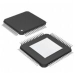 SY89829UHI

The activity of extra discounts on wholesale prices is in full swing…
Please fill in your contact information and we will send you the latest wholesale price list.






