 ChipApex | Global Electronic Components Supplier

SEARCH
Search Product
Search Post
— IC芯片 | 连接器 | 传感器 | 被动器件 —
Search productSearch post
— IC芯片 | 连接器 | 传感器 | 被动器件 —
Consult the customer manager about the wholesale price.
consultation hotline:86-132-6715-2157
email:[email protected]
Contact the product manager for consultation. One-stop consultation is available.
Do you want a lower wholesale price? Please send us your inquiry and we will reply immediately.
SY89830UK4I-TR is listed in the Clock Buffers, Drivers range at ChipApex. The manufacturer field lists Microchip Technology. Its product description is IC CLK BUFFER 2:4 2.5GHZ 16TSSOP. Review the specifications below when checking this part for your BOM.
The SY89830UK4I-TR is a high-speed, differential PECL 1:4 fanout buffer optimized for ultra-low skew applications. It features a 2:1 input MUX and operates within a supply voltage range of 2.5V to 5V. The device guarantees an fMAX greater than 2.5GHz, with within-device skew less than 25ps and propagation delay up to 450ps. It supports LVPECL, PECL, ECL, LVECL, and HSTL logic levels. Operating temperature ranges from –40°C to +85°C. It is housed in a 16-pin TSSOP package.
Verify the 'I' suffix confirms industrial temperature range (-40°C to +85°C) and the 'TR' suffix indicates tape and reel packaging. Confirm RoHS compliance status based on specific manufacturing lot requirements. Ensure proper termination resistors are used as specified in the datasheet for optimal signal integrity.
Select this component when low jitter (<1ps RMS cycle-to-cycle) and minimal skew are critical. Use the integrated 2:1 MUX for redundant clock architectures. Ensure the design accommodates the required output swing and termination schemes for the chosen supply voltage (LVPECL, PECL, or ECL).
This part belongs to Micrel’s Precision Edge family of high-speed timing and distribution components. It serves as a robust solution for distributing differential clock signals across complex digital systems while maintaining strict timing alignment between outputs.
Consult the manufacturer's product line for alternative I/O combinations if different fan-out ratios or logic families are required. Verify pin compatibility before substituting with other devices in the SY89830U series.
The /EN pin forces outputs into a fixed logic state only after the outputs are in a LOW state, eliminating the possibility of generating a "runt" clock pulse during switching.
If only one input pair (IN0 or IN1) is utilized, the unused input pair may be left floating without affecting operation.
The device guarantees within-device skew to be less than 25ps over the full operating temperature and supply voltage range.
Explore related parts through Clock/Timing, Integrated Circuits (ICs), all product categories, ChipApex homepage.
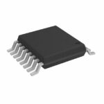 SY89830UK4I-TR

The activity of extra discounts on wholesale prices is in full swing…
Please fill in your contact information and we will send you the latest wholesale price list.






