 ChipApex | Global Electronic Components Supplier

SEARCH
Search Product
Search Post
— IC芯片 | 连接器 | 传感器 | 被动器件 —
Search productSearch post
— IC芯片 | 连接器 | 传感器 | 被动器件 —
Consult the customer manager about the wholesale price.
consultation hotline:86-132-6715-2157
email:[email protected]
Contact the product manager for consultation. One-stop consultation is available.
Do you want a lower wholesale price? Please send us your inquiry and we will reply immediately.
SY89833LMI is listed in the Clock Buffers, Drivers range at ChipApex. The manufacturer field lists Microchip Technology. Its product description is IC CLK BUFFER 1:4 2GHZ 16MLF. Review the specifications below when checking this part for your BOM.
The SY89833LMI is a 3.3V ultra-precision 1:4 LVDS fanout buffer/translator with internal termination, manufactured by Microchip Technology (originally Micrel). It supports DC-to >2GHz throughput with <600ps propagation delay and <20ps within-device skew. The device features a unique internal termination design accessible via the VT pin, allowing interface to various logic standards. It operates from a 3.3V supply (-40°C to +85°C) in a 16-pin QFN package.
Verify the ordering suffix 'I' corresponds to the Industrial temperature range (-40°C to +85°C) as specified in the datasheet's Ordering Information table. Confirm the package type is QFN-16 (3mm x 3mm) and lead finish is NiPdAu Pb-Free. Cross-reference the manufacturer part number SY89833LMG or SY89833LMG TR for equivalent specifications.
Select this component for applications requiring ultra-low skew (<20ps) and high-speed LVDS buffering up to 2GHz. Ensure the design accommodates the 3.3V power supply requirement and utilizes the VT pin for flexible input termination matching different logic standards. Consider the SY89832U if a 2.5V supply is required instead.
The SY89833L belongs to Micrel’s high-speed clock synchronization family. It is designed for ultra-low skew applications and offers flexibility through its patented Any-In input termination architecture. The device integrates internal termination for both inputs and outputs, simplifying board layout for high-speed differential signaling.
The SY89832U provides similar functionality but operates from a 2.5V ±5% supply instead of 3.3V. Verify voltage compatibility and I/O levels before substitution. Consult the Micrel website for other fanout buffers with different I/O combinations if necessary.
It features a patented Any-In input termination design with a VT pin that allows access to the termination network, supporting both DC- and AC-coupled inputs without external resistors.
The device supports a maximum frequency of 2.0 GHz with an output voltage swing of at least 200mV.
The SY89833L guarantees an ultra-low RMS phase jitter of 98 fs over an integration range of 12kHz to 20MHz at an output frequency of 622MHz.
Explore related parts through Clock/Timing, Integrated Circuits (ICs), all product categories, ChipApex homepage.
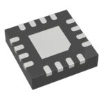 SY89833LMI

The activity of extra discounts on wholesale prices is in full swing…
Please fill in your contact information and we will send you the latest wholesale price list.





