 ChipApex | Global Electronic Components Supplier

SEARCH
Search Product
Search Post
— IC芯片 | 连接器 | 传感器 | 被动器件 —
Search productSearch post
— IC芯片 | 连接器 | 传感器 | 被动器件 —
Consult the customer manager about the wholesale price.
consultation hotline:86-132-6715-2157
email:[email protected]
Contact the product manager for consultation. One-stop consultation is available.
Do you want a lower wholesale price? Please send us your inquiry and we will reply immediately.
SY89841UMG-TR is listed in the Signal Switches, Multiplexers, Decoders range at ChipApex. The manufacturer field lists Microchip Technology. Its product description is IC MULTIPLEXER 1 X 2:1 16MLF. Review the specifications below when checking this part for your BOM.
The SY89841UMG-TR is a Precision LVDS Runt Pulse Eliminator 2:1 multiplexer manufactured by Microchip Technology. It operates from a single 2.5V ±5% supply (2.375V to 2.625V) and supports frequencies up to 1.5GHz. The device features <870ps propagation delay, <150ps rise/fall times, and ultra-low jitter (<1ps rms random). It includes unique RPE logic for glitch-free switchover and Fail-safe Input protection against metastable conditions. Packaged in a 16-pin MLF (3x3mm) surface-mount format.
Verify that the component is sourced from authorized distributors to ensure authenticity. Confirm the package marking matches the specified industrial grade and lead finish. Check for RoHS compliance documentation if required by your manufacturing standards. Ensure the ordering suffix corresponds to the tape and reel configuration needed for your assembly process.
Select this component when glitch-free transition between asynchronous or synchronous clock sources is critical. It is suitable for designs requiring low jitter performance and simplified input interface topologies. Consider the specific power-on reset capacitor requirements for the CAP pin if utilizing the RPE function during system initialization.
This part belongs to Micrel’s Precision Edge product line, now under Microchip Technology following acquisition. It is designed specifically for high-speed digital applications requiring reliable clock distribution. The device integrates advanced isolation and termination features to simplify PCB layout and improve signal integrity in dense electronic systems.
SY89841UMG is the non-tape and reel variant of the same functional device. Verify package compatibility and lead finish specifications when substituting. No other cross-model replacements are confirmed in the provided documentation.
The device uses internal Runt Pulse Eliminator (RPE) logic that controls the switchover sequence in stages, ensuring the output remains stable and free of short cycles or glitches during the transition between primary and secondary clocks.
The Fail-safe Input (FSI) circuit detects when the differential input voltage drops below 100mV and latches the output to the last valid clock state, preventing oscillations or metastable conditions at the output.
Yes, the unique 3-pin input termination architecture allows the device to interface directly with DC-coupled signals (such as CML or LVPECL) without requiring external termination resistor networks or level shifting.
Explore related parts through Logic, Integrated Circuits (ICs), all product categories, ChipApex homepage.
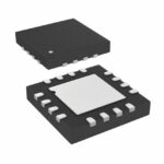 SY89841UMG-TR

The activity of extra discounts on wholesale prices is in full swing…
Please fill in your contact information and we will send you the latest wholesale price list.






