 ChipApex | Global Electronic Components Supplier
SEARCH
Search Product
Search Post
— IC芯片 | 连接器 | 传感器 | 被动器件 —
Search productSearch post
— IC芯片 | 连接器 | 传感器 | 被动器件 —
Consult the customer manager about the wholesale price.
consultation hotline:86-132-6715-2157
email:[email protected]
Contact the product manager for consultation. One-stop consultation is available.
Do you want a lower wholesale price? Please send us your inquiry and we will reply immediately.
The SY89859UMG is a low jitter, low-power, high-speed clock multiplexer featuring an integrated 1:2 differential fanout buffer. It supports input logic levels including CML, LVDS, and PECL, while providing LVPECL outputs. The device operates within a supply voltage range of 2.375V to 3.6V, with typical voltages at 2.5V or 3.3V. It handles maximum input frequencies up to 3500MHz and guarantees data rates to 2.5Gbps. Propagation delay is specified at 0.64ns at maximum load capacitance and 0.85ns absolute. The component functions over an industrial temperature range of -40°C to +85°C.
Verify the specific suffix 'UMG' against the manufacturer's current datasheet to confirm package type and tape/reel specifications. Ensure compatibility with RoHS3 standards if required by your assembly process. Confirm that the operating voltage aligns with your system's 2.375V to 3.6V requirement. Check for any recent Product Change Notifications (PCN) regarding packaging or fabrication site changes.
Select this component when a single high-speed differential clock source needs to be routed to multiple destinations with minimal jitter degradation. It is suitable for systems requiring flexible input format support such as CML, LVDS, or PECL. Consider this part for designs needing integrated termination to simplify the signal path and reduce component count compared to discrete solutions.
This device belongs to the SY89859U series of high-speed multiplexers manufactured by Microchip Technology. It is designed for applications demanding precise timing and low phase noise. The component is part of a broader family of clock management ICs used in telecommunications and computing infrastructure to manage complex clock tree architectures.
Public confirmed substitute part numbers are not available in the provided documentation. Consult official Microchip resources for cross-reference information.
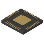 SY89859UMG
The activity of extra discounts on wholesale prices is in full swing…
Please fill in your contact information and we will send you the latest wholesale price list.






