 ChipApex | Global Electronic Components Supplier
SEARCH
Search Product
Search Post
— IC芯片 | 连接器 | 传感器 | 被动器件 —
Search productSearch post
— IC芯片 | 连接器 | 传感器 | 被动器件 —
Consult the customer manager about the wholesale price.
consultation hotline:86-132-6715-2157
email:[email protected]
Contact the product manager for consultation. One-stop consultation is available.
Do you want a lower wholesale price? Please send us your inquiry and we will reply immediately.
The SY89874AUMG is a low-skew, low-jitter clock buffer and programmable divider manufactured by Microchip Technology. It accepts high-speed differential or single-ended inputs (LVTTL, LVCMOS, CML, PECL, LVDS, HSTL) and provides two LVPECL outputs. The device features an integrated programmable divider with ratios of 1, 2, 4, 8, and 16, selectable via S0-S2 pins. Key electrical parameters include a maximum output frequency of 2.5 GHz, propagation delay of 450–760 ps, within-device skew of <15 ps, total jitter <10 ps peak-to-peak, and cycle-to-cycle jitter <1 ps RMS. It operates on a 2.375V to 3.63V supply in a 16-pin QFN package.
Verify the ordering suffix 'UMG' corresponds to the 16-Lead 3 mm x 3 mm QFN package, -40°C to +85°C temperature range, and NiPdAu lead-free finish. Confirm packing quantity requirements; standard tubes contain 110 units, while tape and reel options are available as SY89874AUMG-TR with 1,000 units per reel. Ensure compatibility with RoHS3 standards.
Select the SY89874AUMG when a 1:2 fanout with programmable division is required for frequencies up to 2.5 GHz. Use this part for AC-coupled or DC-coupled applications supporting multiple logic standards. For wider differential input voltage ranges suitable for low-offset signals, consider the SY89874U variant instead. Ensure power supply decoupling with 0.1 μF and 0.01 μF capacitors near VCC pins.
This component belongs to the Precision Edge® series of clock drivers and distributors from Microchip Technology. It is functionally related to the SY89874AU base model but specifies the specific package and environmental ratings in its full part number. It serves as a frequency translator and buffer in high-speed digital systems requiring precise timing distribution.
Public confirmed substitute part numbers are not provided in the source material. Designers should verify pin compatibility and electrical specifications if considering alternative vendors or family members like the SY89874U for different input range requirements.
The divide ratio (1, 2, 4, 8, or 16) is selected using the S0, S1, and S2 pins. These pins accept LVTTL/CMOS logic levels and have internal 25 kΩ pull-up resistors. Leaving them unconnected results in a divide-by-16 mode.
The VT pin provides access to the internal termination network. For CML or LVDS inputs, it should be left floating. For other logic standards, it connects to specific termination circuits to ensure proper signal integrity for both DC and AC coupling.
The /RESET pin asynchronously resets the divider in divide modes (2, 4, 8, 16). In pass-through mode (divide by 1), it acts as a synchronous enable/disable function, turning outputs off on the next falling edge of the input clock.
Yes, unused PECL outputs may be left floating without impacting jitter performance. However, if terminating unused I/O for balance, specific resistor networks (e.g., R3=1kΩ, R4=1.6kΩ for 3.3V) are recommended.
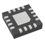 SY89874AUMG
The activity of extra discounts on wholesale prices is in full swing…
Please fill in your contact information and we will send you the latest wholesale price list.





