 ChipApex | Global Electronic Components Supplier
SEARCH
Search Product
Search Post
— IC芯片 | 连接器 | 传感器 | 被动器件 —
Search productSearch post
— IC芯片 | 连接器 | 传感器 | 被动器件 —
Consult the customer manager about the wholesale price.
consultation hotline:86-132-6715-2157
email:[email protected]
Contact the product manager for consultation. One-stop consultation is available.
Do you want a lower wholesale price? Please send us your inquiry and we will reply immediately.
The SY89874UMG is a low-skew, low-jitter integrated circuit featuring a programmable clock divider and a 1:2 fanout buffer. It accepts high-speed differential inputs (CML, LVDS, PECL, HSTL) and divides the frequency by ratios of 2, 4, 8, or 16, or passes through the reference clock. The device provides two differential LVPECL outputs with guaranteed AC performance up to 2.5 GHz maximum output toggle frequency. Key electrical parameters include a supply voltage range of 2.375V to 3.63V, within-device skew of less than 15 ps, total jitter under 10 ps peak-to-peak, and cycle-to-cycle jitter under 1 ps RMS.
Verify the ordering suffix 'TR' if tape and reel packaging is required instead of the standard tube. Confirm that the exposed pad on the QFN package is soldered to a ground plane for proper thermal management and electrical connection. Ensure the application voltage aligns with the specified 2.5V or 3.3V operating ranges.
Select this component when a single differential input must be divided and distributed to two LVPECL loads. Verify compatibility with the source signal standard (CML, LVDS, PECL, or HSTL) and ensure the required division ratio matches the S0-S2 pin configuration. Check that the system power supply falls within the 2.375V to 3.63V window.
This device belongs to the SY89874 family, specifically designed as a 2.5 GHz Any-Diff-In-to-LVPECL Programmable Clock Divider/Fanout Buffer. It utilizes a 16-pin 3 mm x 3 mm QFN package. The 'UMG' suffix indicates a 2.5V/3.3V input voltage capability, a 3 mm x 3 mm QFN-16 package, and an operating temperature range of –40°C to +85°C.
Public confirmed substitute part numbers are not available in the provided documentation.
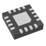 SY89874UMG
The activity of extra discounts on wholesale prices is in full swing…
Please fill in your contact information and we will send you the latest wholesale price list.





