 ChipApex | Global Electronic Components Supplier
SEARCH
Search Product
Search Post
— IC芯片 | 连接器 | 传感器 | 被动器件 —
Search productSearch post
— IC芯片 | 连接器 | 传感器 | 被动器件 —
Consult the customer manager about the wholesale price.
consultation hotline:86-132-6715-2157
email:[email protected]
Contact the product manager for consultation. One-stop consultation is available.
Do you want a lower wholesale price? Please send us your inquiry and we will reply immediately.
The SYA75603BTWLVAO is an automotive-grade PCIe clock buffer featuring two ultra-low additive jitter outputs. It supports PCIe Gen 1 through 5 with frequencies up to 250 MHz and delivers 10 fs peak-to-peak additive jitter for Gen 5 applications. The device incorporates embedded 100Ω differential termination resistors at the LP-HCSL outputs, eliminating external components. It accepts DC-coupled HCSL or AC-coupled PECL/LVDS/CML inputs and provides individual glitch-free output enable control via active-low pins. Powered by a single supply of 1.8V, 2.5V, or 3.3V (±10%), it includes internal LDOs for superior power noise rejection.
Verify that the 'B' suffix indicates the specific variant with 100Ω embedded output termination resistors. Confirm the 'TWL' package designation corresponds to the 16-lead 3 mm x 3 mm VQFN form factor. Ensure the 'VAO' suffix aligns with the required automotive qualification standards for the target application environment.
Select this component when a two-channel fanout buffer is required for high-speed PCIe interfaces in automotive environments. The choice between the 'A' and 'B' variants depends on whether the design requires 85Ω or 100Ω embedded termination. This part is suitable for designs needing independent output gating without introducing glitches during state transitions.
This device belongs to the SYA75603A/B family of PCIe clock buffers designed for automotive reliability. It shares the same core architecture and packaging as the SYA75603A but differs in its output impedance characteristics. The model is specifically engineered to meet the stringent jitter and power supply noise requirements defined by the PCIe Card Electro Mechanical Specification.
Public confirmed substitute part numbers are not available in the provided documentation.
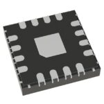 SYA75603BTWLVAO
The activity of extra discounts on wholesale prices is in full swing…
Please fill in your contact information and we will send you the latest wholesale price list.





