 ChipApex | Global Electronic Components Supplier
SEARCH
Search Product
Search Post
— IC芯片 | 连接器 | 传感器 | 被动器件 —
Search productSearch post
— IC芯片 | 连接器 | 传感器 | 被动器件 —
Consult the customer manager about the wholesale price.
consultation hotline:86-132-6715-2157
email:[email protected]
Contact the product manager for consultation. One-stop consultation is available.
Do you want a lower wholesale price? Please send us your inquiry and we will reply immediately.
The SYA75604ATWLVAO is an automotive-grade, four-output PCIe clock buffer designed for ultra-low additive jitter applications. It supports frequencies up to 250 MHz and complies with PCIe Gen 1 through Gen 5 standards. The device features Low Power HCSL (LP-HCSL) outputs with embedded 85Ω differential termination resistors. It accepts DC-coupled HCSL inputs as well as AC-coupled PECL, LVDS, and CML signals. Operating voltage ranges from 1.62 V to 3.63 V, supporting 1.8V, 2.5V, and 3.3V supplies with ±10% tolerance. The component includes individual glitch-free output enable pins and operates within a temperature range of –40°C to +105°C.
Verify that the specific ordering suffix matches the required package media type. The 'TWL' suffix indicates a 16-lead 3 mm x 3 mm VQFN package with wettable flanks. The '-VAO' suffix denotes standard automotive grade compliance. Confirm whether the tube or reel configuration is required for the manufacturing process, as these are distinct part variants within the same family.
Select the SYA75604A variant specifically when 85Ω embedded termination is required; the SYA75604B variant provides 100Ω termination. Ensure the design utilizes the 3 mm x 3 mm VQFN footprint compatible with the 16-lead package outline. Verify that the input signal source supports the specified voltage levels and coupling methods, as the device accepts both single-ended and differential inputs.
This component belongs to the SYA75603A/B and SYA75604A/B family of automotive PCIe clock buffers. It shares core electrical characteristics with the two-output SYA75603A/B but provides four independent outputs. All parts in this series are designed to meet automotive reliability standards and support the full spectrum of PCIe generations from 1.0 to 5.0.
Publicly confirmed substitute part numbers are not available in the provided documentation. Designers should consult Microchip technical support for cross-reference information regarding alternative timing solutions.
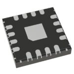 SYA75604ATWLVAO
The activity of extra discounts on wholesale prices is in full swing…
Please fill in your contact information and we will send you the latest wholesale price list.




