 ChipApex | Global Electronic Components Supplier

SEARCH
Search Product
Search Post
— IC芯片 | 连接器 | 传感器 | 被动器件 —
Search productSearch post
— IC芯片 | 连接器 | 传感器 | 被动器件 —
Consult the customer manager about the wholesale price.
consultation hotline:86-132-6715-2157
email:[email protected]
Contact the product manager for consultation. One-stop consultation is available.
Do you want a lower wholesale price? Please send us your inquiry and we will reply immediately.
TC7135CPI is listed in the ADCs/DACs - Special Purpose range at ChipApex. The manufacturer field lists Microchip Technology. Its product description is IC DRVR 7 SEG 4 1/2 DIGIT 28DIP. Review the specifications below when checking this part for your BOM.
The TC7135CPI is a 4-1/2 digit dual-slope integrating analog-to-digital converter (ADC) manufactured by Microchip Technology in a 28-pin PDIP package. It provides 50 ppm resolution with a maximum nonlinearity error of ±1 count and an auto-zero cycle that reduces zero error to below 10 µV. The device features multiplexed BCD data outputs, TTL-compatible logic levels, and control signals including BUSY, STROBE, and RUN/HOLD for microprocessor interfacing. Key electrical specifications include a typical input leakage current of 1 pA, a zero reading drift of 0.5 µV/°C, and operation with ±5V power supplies.
Verify the component matches the specific 28-pin PDIP package configuration. Confirm that the operating environment stays within the specified 0°C to +70°C temperature range. Ensure external reference components meet stability requirements for absolute accuracy measurements.
Select this component for applications requiring high precision DC measurements where low drift and noise immunity are critical. The dual-slope design offers inherent rejection of line frequency noise when clock frequencies are appropriately chosen. Consider the 1 pA input leakage for high-impedance source applications.
The TC7135 is part of Microchip's family of integrating A/D converters designed for high-accuracy measurement systems. The 'CPI' suffix denotes the commercial temperature range variant housed in a standard 28-pin plastic dual in-line package, distinguishing it from surface-mount MQFP or PLCC options.
Direct pin-for-pin replacements should be verified against the 28-pin PDIP footprint. Alternative ADCs must support dual-slope integration principles and compatible multiplexed BCD output timing to maintain existing circuit functionality without redesign.
If the input signal causes the reference voltage integration time to exceed 20,000 clock pulses, the OVERRANGE output goes high. In this state, all digit drive signals are held low, causing the display to blink visually.
The ANALOG COMMON pin serves as the reference point for REF IN and the -INPUT return during auto-zero and de-integration phases. Tying it to the same point as -INPUT removes common-mode voltage from the converter.
The conversion rate depends on the clock frequency applied to the CLOCK IN pin. For example, a 120 kHz clock results in approximately 3 conversions per second, while a 100 kHz clock yields 2.5 conversions per second.
Explore related parts through Data Acquisition, Integrated Circuits (ICs), all product categories, ChipApex homepage.
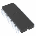 TC7135CPI

The activity of extra discounts on wholesale prices is in full swing…
Please fill in your contact information and we will send you the latest wholesale price list.






