 ChipApex | Global Electronic Components Supplier

SEARCH
Search Product
Search Post
— IC芯片 | 连接器 | 传感器 | 被动器件 —
Search productSearch post
— IC芯片 | 连接器 | 传感器 | 被动器件 —
Consult the customer manager about the wholesale price.
consultation hotline:86-132-6715-2157
email:[email protected]
Contact the product manager for consultation. One-stop consultation is available.
Do you want a lower wholesale price? Please send us your inquiry and we will reply immediately.
The TC74LCX125FK is a low-voltage quad bus buffer manufactured by Toshiba Semiconductor and Storage. It operates within a supply voltage range of 1.65 V to 3.6 V, with inputs and outputs tolerant up to 5.5 V. The device features four non-inverting buffers with three-state outputs controlled by an OE input. Key electrical parameters include a maximum propagation delay of 6.0 ns at 3.3 V, minimum output currents of ±24 mA, and power-down protection on all pins. It is available in SOP-14 and VSSOP-14 packages.
Verify the specific package suffix (FK indicates VSSOP) against the required footprint. Confirm RoHS compliance status directly with the manufacturer or authorized distributors, as datasheet documentation regarding environmental certifications may vary by production batch. Ensure the design accounts for the specified operating temperature range of -40°C to 85°C.
Select this component when a quad bus buffer with 5-V tolerance is required for low-voltage applications. It serves as a pin-compatible replacement for various 74-series drivers such as 74AC/VHC/HC/F/ALS/LS types. Consider the VSSOP package for space-constrained designs compared to the standard SOP option.
This part belongs to the TC74LCX series of low-voltage CMOS digital integrated circuits. The LCX family is designed specifically for low-power, high-speed applications in portable and battery-operated devices. The 125 variant specifically denotes a quad buffer with three-state outputs, distinguishing it from inverters or transceivers within the same logical family.
The datasheet explicitly states pin and function compatibility with the 74AC, 74VHC, 74HC, 74F, 74ALS, and 74LS 125 type devices. These can be considered direct functional substitutes if voltage levels and speed requirements align with the LCX specifications.
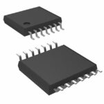 TC74LCX125FK(EL,K)

The activity of extra discounts on wholesale prices is in full swing…
Please fill in your contact information and we will send you the latest wholesale price list.





