 ChipApex | Global Electronic Components Supplier
SEARCH
Search Product
Search Post
— IC芯片 | 连接器 | 传感器 | 被动器件 —
Search productSearch post
— IC芯片 | 连接器 | 传感器 | 被动器件 —
Consult the customer manager about the wholesale price.
consultation hotline:86-132-6715-2157
email:[email protected]
Contact the product manager for consultation. One-stop consultation is available.
Do you want a lower wholesale price? Please send us your inquiry and we will reply immediately.
The TC74LCX540F is a low-voltage octal bus buffer with inverted logic and 5-V tolerant inputs and outputs. It operates within a supply voltage range of 1.65 V to 3.6 V, achieving a maximum propagation delay of 6.5 ns at 3.0 V to 3.6 V. The device provides an output current capability of 24 mA minimum at 3.0 V. It features two active-low output enables (1OE and 2OE) for three-state control and includes power-down protection on all inputs and outputs.
Verify the specific package variant required, as the part number suffix indicates either SOP or VSSOP packaging. Confirm that the application environment supports the specified 1.65 V to 3.6 V operating voltage range. Ensure input signals remain within the 0 V to 5.5 V tolerance limits to maintain device integrity. Check for RoHS compliance requirements if applicable to the target assembly process.
Select this component when designing systems requiring interface between 3.3 V logic and 5 V tolerant buses. The inverted logic configuration distinguishes it from non-inverting variants like the TC74LCX541. Consider the 24 mA drive strength for driving moderate capacitive loads. Verify that the available packages (SOP or VSSOP) fit the board layout constraints.
This device belongs to the Toshiba LCX series of advanced high-speed CMOS logic integrated circuits. It is functionally compatible with standard 74 series devices such as the 74AC, 74VHC, 74HC, and 74LS types, facilitating direct replacement in existing designs. The octal buffer architecture allows for the buffering of eight independent data lines simultaneously.
Functionally equivalent parts include the TC74LCX541 for non-inverting applications. For higher speed requirements, consider the TC74AC540 series. For standard 5 V operation, the TC74HC540 may be used, though voltage compatibility differs.
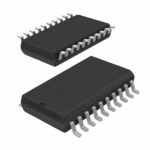 TC74LCX540F(EL,K,F
The activity of extra discounts on wholesale prices is in full swing…
Please fill in your contact information and we will send you the latest wholesale price list.




