 ChipApex | Global Electronic Components Supplier
SEARCH
Search Product
Search Post
— IC芯片 | 连接器 | 传感器 | 被动器件 —
Search productSearch post
— IC芯片 | 连接器 | 传感器 | 被动器件 —
Consult the customer manager about the wholesale price.
consultation hotline:86-132-6715-2157
email:[email protected]
Contact the product manager for consultation. One-stop consultation is available.
Do you want a lower wholesale price? Please send us your inquiry and we will reply immediately.
The TC74VHC367FTEL is a hex bus buffer fabricated with silicon gate C2MOS technology. It contains six non-inverting buffers controlled by two enable inputs (1G and 2G). Outputs enter a high-impedance state when enabled inputs are held high. The device supports a supply voltage range of 2.0 V to 5.5 V, with input voltages tolerating up to 5.5 V regardless of the supply level. Propagation delay is typically 3.8 ns at 5 V. Quiescent current is 4 μA maximum at 25°C. Noise immunity is defined as 28% of VCC minimum.
Verify the specific package suffix against the datasheet to confirm physical dimensions and weight. Ensure the ordering code matches the required TSSOP or other variant. Confirm RoHS compliance status directly with Toshiba Semiconductor and Storage representatives prior to procurement. Review the restrictions on product use for unintended applications.
Select this component for designs requiring hex bus buffering with independent control groups. The dual enable inputs allow flexible partitioning of the six buffers. Verify that the 5.5 V input tolerance meets system requirements for interfacing different voltage domains. Check propagation delay specifications against the target clock frequencies in the specific operating temperature range.
This part belongs to the TC74VHC367/368 series of advanced high-speed CMOS logic devices. It is functionally compatible with the 74ALS367/368 standard. The FTEL designation indicates a specific surface-mount package variant within the broader family of hex bus buffers produced by Toshiba Semiconductor and Storage.
Direct substitute part numbers include SN74AHC367PWR from Texas Instruments.
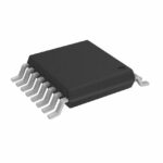 TC74VHC367FTEL
The activity of extra discounts on wholesale prices is in full swing…
Please fill in your contact information and we will send you the latest wholesale price list.





