 ChipApex | Global Electronic Components Supplier
SEARCH
Search Product
Search Post
— IC芯片 | 连接器 | 传感器 | 被动器件 —
Search productSearch post
— IC芯片 | 连接器 | 传感器 | 被动器件 —
Consult the customer manager about the wholesale price.
consultation hotline:86-132-6715-2157
email:[email protected]
Contact the product manager for consultation. One-stop consultation is available.
Do you want a lower wholesale price? Please send us your inquiry and we will reply immediately.
The TC7MB3257CFK-EL(M) is a low capacitance CMOS quad 1-of-2 multiplexer/demultiplexer manufactured by Toshiba Semiconductor and Storage. It operates within a supply voltage range of 4.0 to 5.5 V and functions across an operating temperature range of -40 to 85 °C. The device features four independent multiplexers with common select (S) and output enable (OE) inputs. Key electrical characteristics include a typical on-resistance (RON) of 3 Ω at VCC=4.5V and a switch-on capacitance (CI/O) of 8.5 pF at VCC=5V. The component is housed in a 16-pin VSSOP package.
Verify the specific suffix EL(M) against official Toshiba documentation to confirm the exact packaging configuration and manufacturing lot details. Ensure that the procurement channel provides valid traceability for the semiconductor components. Confirm RoHS compliance status through the manufacturer's latest environmental declarations before finalizing orders.
Select this component when a quad 1-of-2 multiplexer is required for 5V logic systems with strict low capacitance constraints. The VSSOP16 package is suitable for space-constrained surface mount designs. Consider the 3 Ω typical on-resistance for signal integrity requirements. Verify compatibility with existing TTL-level control signals if interfacing with legacy logic families.
This part belongs to the TC7MB3257 series of low capacitance CMOS digital integrated circuits. It serves as a specialized signal switching solution designed for applications where signal integrity and speed are critical. The device integrates four independent channels, providing a compact alternative to discrete switching solutions while maintaining robust ESD protection and power-down safety features.
The datasheet notes pin compatibility with the TC7MB3257FT/FK variants. These parts share identical functionality and pin assignments but differ in physical package types (TSSOP or VQON). Verify package dimensions and thermal characteristics when substituting between these specific form factors.
When the OE input is held at a high level, the switches remain open regardless of the select input states, resulting in a high-impedance state between the switches.
The device offers an ESD performance of ≥ ±200 V for the machine model and ≥ ±2000 V for the human body model.
No, unused control pin inputs must be tied to either VCC or GND to ensure proper operation and prevent undefined states.
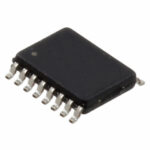 TC7MB3257CFK-EL(M)
The activity of extra discounts on wholesale prices is in full swing…
Please fill in your contact information and we will send you the latest wholesale price list.






