 ChipApex | Global Electronic Components Supplier
SEARCH
Search Product
Search Post
— IC芯片 | 连接器 | 传感器 | 被动器件 —
Search productSearch post
— IC芯片 | 连接器 | 传感器 | 被动器件 —
Consult the customer manager about the wholesale price.
consultation hotline:86-132-6715-2157
email:[email protected]
Contact the product manager for consultation. One-stop consultation is available.
Do you want a lower wholesale price? Please send us your inquiry and we will reply immediately.
The TC7MB3257CFT-EL(M) is a low capacitance CMOS quad 1-of-2 multiplexer/demultiplexer manufactured by Toshiba Semiconductor and Storage. It operates within a supply voltage range of 4.0 to 5.5 V and supports an operating temperature from -40 to 85 °C. The device features four independent channels with common select (S) and output enable (OE) inputs. Key electrical parameters include a typical on-resistance (RON) of 3 Ω at VCC=4.5V and a switch-on capacitance (CI/O) of 8.5 pF at VCC=5V. ESD protection ratings are ±200 V for the machine model and ±2000 V for the human body model.
Verify the specific package variant required, as the base part number covers TSSOP16, VSSOP16, and VQON16 options. Confirm RoHS compliance status directly with the manufacturer or authorized distributors, as environmental declarations may vary by production batch. Ensure that the ordering suffix matches the desired physical footprint and tape-and-reel specifications for automated assembly processes.
Select this component when low signal distortion and fast switching speeds are critical due to its low capacitance profile. Ensure the system supply voltage remains within the 4.0 V to 5.5 V operating range to maintain specified on-resistance values. Consider the ESD protection levels if the application involves frequent handling or exposure to electrostatic discharge risks without additional circuit safeguards.
This device belongs to the TC7MBL series of low capacitance bus switches and multiplexers designed for space-constrained applications. It serves as a functional alternative to standard logic switches where signal integrity is paramount. The quad configuration allows for efficient management of multiple data paths using a minimal number of control pins, optimizing board layout complexity.
The datasheet notes pin compatibility with the TC7MB3257FT and TC7MB3257FK variants. Verify package dimensions and weight differences if substituting between TSSOP, VSSOP, or VQON footprints to ensure mechanical fit.
When the OE input is held at a high level, the switches remain open regardless of the select input state, creating a high-impedance state between the terminals.
The absolute maximum power dissipation rating is 180 mW.
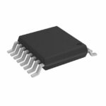 TC7MB3257CFT-EL(M)
The activity of extra discounts on wholesale prices is in full swing…
Please fill in your contact information and we will send you the latest wholesale price list.






