 ChipApex | Global Electronic Components Supplier
SEARCH
Search Product
Search Post
— IC芯片 | 连接器 | 传感器 | 被动器件 —
Search productSearch post
— IC芯片 | 连接器 | 传感器 | 被动器件 —
Consult the customer manager about the wholesale price.
consultation hotline:86-132-6715-2157
email:[email protected]
Contact the product manager for consultation. One-stop consultation is available.
Do you want a lower wholesale price? Please send us your inquiry and we will reply immediately.
The TC7MBL3257CFK is a low-voltage, low-capacitance CMOS digital integrated circuit functioning as a 4-bit 1-of-2 multiplexer/demultiplexer. It operates within a supply voltage range of 1.65 V to 3.6 V and supports an operating temperature range from -40 °C to +85 °C. The device features four independent switching circuits with common select (S) and output enable (OE) inputs. Key electrical parameters include a typical ON-resistance of 8.5 Ω at 3.0 V and a typical ON capacitance of 8 pF. Maximum propagation delay times are specified up to 11 ns depending on the supply voltage.
Verify the specific ordering suffix and package variant against the manufacturer's official documentation before procurement. Confirm that the selected part number matches the required pin configuration and marking code. Ensure compliance with RoHS directives and environmental regulations applicable to your region. Review the absolute maximum ratings and derating guidelines to guarantee long-term operational reliability under intended load conditions.
Select this component when designing circuits requiring low-voltage operation between 1.65 V and 3.6 V. Consider the 8.5 Ω typical ON-resistance and 8 pF ON-capacitance for high-speed signal integrity requirements. Evaluate the 16-pin VSSOP package dimensions for PCB layout constraints. Ensure the application does not exceed the specified operating temperature range of -40 °C to +85 °C.
This device belongs to the TC7MBL series of CMOS digital logic ICs manufactured by Toshiba Semiconductor and Storage. It is designed for low-power, low-voltage applications where minimal signal degradation is critical. The component utilizes silicon monolithic technology and is housed in a compact surface-mount package suitable for space-constrained designs.
Consult the official Toshiba datasheet for verified substitute part numbers or compatible alternatives within the same product family. Cross-reference pinouts and electrical specifications to ensure functional equivalence. Verify package compatibility and thermal performance before implementing any replacement.
When the OE input is held at a high level, the switches remain open regardless of the select input state, placing the outputs in a high-impedance state.
The Select input determines which input port (B1 or B2) is connected to the A port. A low level connects A to B1, while a high level connects A to B2.
Yes, the TC7MBL3257CFK includes power-down protection for all inputs, including OE, S, and I/O, to prevent excessive leakage current when the device is powered off.
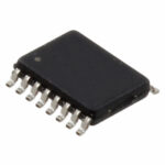 TC7MBL3257CFK(EL)
The activity of extra discounts on wholesale prices is in full swing…
Please fill in your contact information and we will send you the latest wholesale price list.





