 ChipApex | Global Electronic Components Supplier
SEARCH
Search Product
Search Post
— IC芯片 | 连接器 | 传感器 | 被动器件 —
Search productSearch post
— IC芯片 | 连接器 | 传感器 | 被动器件 —
Consult the customer manager about the wholesale price.
consultation hotline:86-132-6715-2157
email:[email protected]
Contact the product manager for consultation. One-stop consultation is available.
Do you want a lower wholesale price? Please send us your inquiry and we will reply immediately.
The TC7MPB9307FK(EL) is a CMOS 8-bit dual-supply bus switch designed for low-voltage and low-power applications. It facilitates bidirectional level shifting between two nodes operating at different voltage levels. The device supports VCCA ranges of 1.65 V to 5.0 V and VCCB ranges of 2.3 V to 5.5 V. Key electrical parameters include a maximum ON-resistance of 16 Ω, a maximum propagation delay of 1.2 ns, and a maximum quiescent supply current of 10 µA. It operates within a temperature range of -40°C to +85°C and is housed in a VSSOP-20 package.
Verify the specific ordering suffix matches the required packaging format, as variations exist between reel, cut tape, and MouseReel options. Confirm RoHS compliance status through official Toshiba documentation prior to integration. Ensure design accounts for the absolute maximum ratings, particularly regarding supply voltage limits and power dissipation constraints under varying thermal conditions.
Select this component when an 8-bit wide bus interface is required between domains with distinct voltage rails. The device is suitable for designs prioritizing low static power consumption and high-speed signal integrity. Consider the VSSOP-20 package dimensions for PCB layout constraints. Ensure the application does not exceed the specified operating temperature range or require functionality beyond the single enable control architecture.
This part belongs to the TC7MPB series of CMOS digital integrated circuits manufactured by Toshiba Semiconductor and Storage. It is specifically categorized as a low-voltage, low-power dual-supply bus switch. The family focuses on providing flexible interfacing solutions for modern electronic systems requiring efficient voltage level translation across multiple data lines.
Public confirmed substitute part numbers are not available in the provided documentation. Consult Toshiba sales representatives for alternative components with compatible pinouts and electrical specifications if this specific model is unavailable.
Bidirectional level shifting is enabled by adding external pull-up resistors between the An/Bn data lines and the respective VCCA/VCCB supplies. There are no restrictions on the relative magnitude of the An and Bn voltages.
The Output Enable (OE) input controls the connection or isolation of the two bus systems. When OE is Low, the switch connects An to Bn; when High, the switch disconnects them. This control is common for all eight bits.
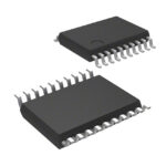 TC7MPB9307FK(EL)
The activity of extra discounts on wholesale prices is in full swing…
Please fill in your contact information and we will send you the latest wholesale price list.






