 ChipApex | Global Electronic Components Supplier
SEARCH
Search Product
Search Post
— IC芯片 | 连接器 | 传感器 | 被动器件 —
Search productSearch post
— IC芯片 | 连接器 | 传感器 | 被动器件 —
Consult the customer manager about the wholesale price.
consultation hotline:86-132-6715-2157
email:[email protected]
Contact the product manager for consultation. One-stop consultation is available.
Do you want a lower wholesale price? Please send us your inquiry and we will reply immediately.
The TC7MPB9326FT(EL) is a CMOS dual multiplexer/demultiplexer bus switch designed for low voltage and low power applications. It provides bidirectional level-shifting interfaces between nodes operating at different voltage levels, supporting VCCA ranges of 1.65 to 5.0 V and VCCB ranges of 2.3 to 5.5 V. The device features an active high Output Enable (OE) pin that isolates bus lines when disabled. It includes power-down protection on the OE input, which is 5.5 V tolerant. The package is TSSOP14.
Verify the specific ordering suffix FT corresponds to the TSSOP14 package configuration required for your design. Confirm that the active high OE logic aligns with your system control signals, as the companion TC7MPB9327 utilizes active low enable. Ensure voltage levels remain within specified operating ranges to maintain reliability.
Select this component when designing interfaces between disparate voltage domains such as 1.8V, 2.5V, 3.3V, and 5.0V systems. The dual multiplexer structure supports two independent data paths sharing a common select input. Consider the TSSOP14 footprint constraints and verify that the 5.5 V tolerant OE input matches your control logic requirements.
This part belongs to the TC7MPB9326/9327 series of low voltage dual SPDT supply bus switches manufactured by Toshiba Semiconductor and Storage. The series complements other bus switch solutions by offering dedicated level-shifting capabilities with integrated power-down protection. The FT suffix specifically denotes the TSSOP14 surface-mount package variant.
The TC7MPB9327FK or TC7MPB9327FT serves as a functional substitute with identical electrical characteristics but utilizes an active low Output Enable (OE) pin instead of active high. Verify control logic polarity compatibility before substitution.
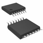 TC7MPB9326FT(EL)
The activity of extra discounts on wholesale prices is in full swing…
Please fill in your contact information and we will send you the latest wholesale price list.






